- 您现在的位置:买卖IC网 > PDF目录17007 > USB-I2C/LIN-CONV-Z (Analog Devices Inc)USB TO I2C/LIN CONV BOARD PDF资料下载
参数资料
| 型号: | USB-I2C/LIN-CONV-Z |
| 厂商: | Analog Devices Inc |
| 文件页数: | 93/104页 |
| 文件大小: | 0K |
| 描述: | USB TO I2C/LIN CONV BOARD |
| 标准包装: | 1 |
| 附件类型: | 适配器板 |
| 适用于相关产品: | ARM7TDMI? |
第1页第2页第3页第4页第5页第6页第7页第8页第9页第10页第11页第12页第13页第14页第15页第16页第17页第18页第19页第20页第21页第22页第23页第24页第25页第26页第27页第28页第29页第30页第31页第32页第33页第34页第35页第36页第37页第38页第39页第40页第41页第42页第43页第44页第45页第46页第47页第48页第49页第50页第51页第52页第53页第54页第55页第56页第57页第58页第59页第60页第61页第62页第63页第64页第65页第66页第67页第68页第69页第70页第71页第72页第73页第74页第75页第76页第77页第78页第79页第80页第81页第82页第83页第84页第85页第86页第87页第88页第89页第90页第91页第92页当前第93页第94页第95页第96页第97页第98页第99页第100页第101页第102页第103页第104页
Data Sheet
ADuC7019/20/21/22/24/25/26/27/28/29
Rev. F | Page 89 of 104
Table 191. T3CON MMR Bit Descriptions
Bit
Value
Description
15:9
Reserved.
8
Count up. Set by user for Timer3 to count up.
Cleared by user for Timer3 to count down by
default.
7
Timer3 enable bit. Set by user to enable Timer3.
Cleared by user to disable Timer3 by default.
6
Timer3 mode. Set by user to operate in
periodic mode. Cleared by user to operate
in free-running mode. Default mode.
5
Watchdog mode enable bit. Set by user to
enable watchdog mode. Cleared by user to
disable watchdog mode by default.
4
Secure clear bit. Set by user to use the secure
clear option. Cleared by user to disable the
secure clear option by default.
3:2
Prescale.
00
Source Clock/1 by default.
01
Source Clock/16.
10
Source Clock/256.
11
Undefined. Equivalent to 00.
1
Watchdog IRQ option bit. Set by user to
produce an IRQ instead of a reset when
the watchdog reaches 0. Cleared by user to
disable the IRQ option.
0
Reserved.
Table 192. T3CLRI Register
Name
Address
Default Value
Access
T3CLRI
0xFFFF036C
0x00
W
T3CLRI is an 8-bit register. Writing any value to this register on
successive occassions clears the Timer3 interrupt in normal
mode or resets a new timeout period in watchdog mode.
Note that the user must perform successive writes to this
register to ensure resetting the timeout period.
Secure Clear Bit (Watchdog Mode Only)
The secure clear bit is provided for a higher level of protection.
When set, a specific sequential value must be written to T3CLRI
to avoid a watchdog reset. The value is a sequence generated
by the 8-bit linear feedback shift register (LFSR) polynomial =
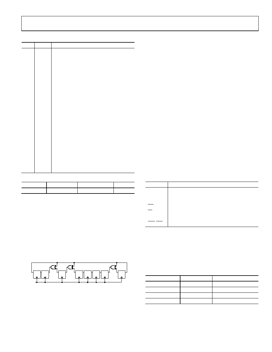
X8 + X6 + X5 + X + 1, as shown in Figure 81.
049
55
-03
8
CLOCK
QD
4
QD
5
QD
3
QD
7
QD
6
QD
2
QD
1
QD
0
Figure 81. 8-Bit LFSR
The initial value or seed is written to T3CLRI before entering
watchdog mode. After entering watchdog mode, a write to
T3CLRI must match this expected value. If it matches, the LFSR
is advanced to the next state when the counter reload occurs. If
it fails to match the expected state, a reset is immediately
generated, even if the count has not yet expired.
The value 0x00 should not be used as an initial seed due to
the properties of the polynomial. The value 0x00 is always
guaranteed to force an immediate reset. The value of the LFSR
cannot be read; it must be tracked/generated in software.
The following is an example of a sequence:
1.
Enter initial seed, 0xAA, in T3CLRI before starting Timer3
in watchdog mode.
2.
Enter 0xAA in T3CLRI; Timer3 is reloaded.
3.
Enter 0x37 in T3CLRI; Timer3 is reloaded.
4.
Enter 0x6E in T3CLRI; Timer3 is reloaded.
5.
Enter 0x66. 0xDC was expected; the watchdog resets the chip.
EXTERNAL MEMORY INTERFACING
The ADuC7026 and ADuC7027 are the only models in their
series that feature an external memory interface. The external
memory interface requires a larger number of pins. This is why
it is only available on larger pin count packages. The XMCFG
MMR must be set to 1 to use the external port.
Although 32-bit addresses are supported internally, only the
lower 16 bits of the address are on external pins.
The memory interface can address up to four 128 kB blocks of
asynchronous memory (SRAM or/and EEPROM).
The pins required for interfacing to an external memory are
shown in Table 193.
Table 193. External Memory Interfacing Pins
Pin
Function
AD[16:1]
Address/data bus
A16
Extended addressing for 8-bit memory only
MS[3:0]
Memory select
WS
Write strobe
RS
Read strobe
AE
Address latch enable
BHE, BLE
Byte write capability
There are four external memory regions available, as described
in Table 194. Associated with each region are the MS[3:0] pins.
These signals allow access to the particular region of external
memory. The size of each memory region can be 128 kB maxi-
mum, 64 k × 16 or 128 k × 8. To access 128 k with an 8-bit
memory, an extra address line (A16) is provided (see the example
in Figure 82). The four regions are configured independently.
Table 194. Memory Regions
Address Start
Address End
Contents
0x10000000
0x1000FFFF
External Memory 0
0x20000000
0x2000FFFF
External Memory 1
0x30000000
0x3000FFFF
External Memory 2
0x40000000
0x4000FFFF
External Memory 3
Each external memory region can be controlled through three
MMRs: XMCFG, XMxCON, and XMxPAR.
相关PDF资料 |
PDF描述 |
|---|---|
| HBM10DSEI-S13 | CONN EDGECARD 20POS .156 EXTEND |
| EBC35DCSD-S288 | CONN EDGECARD 70POS .100 EXTEND |
| HBM15DRYN-S13 | CONN EDGECARD 30POS .156 EXTEND |
| RBC17DRES-S13 | CONN EDGECARD 34POS .100 EXTEND |
| HBM15DRYH-S13 | CONN EDGECARD 30POS .156 EXTEND |
相关代理商/技术参数 |
参数描述 |
|---|---|
| USB-I2C-SS | 功能描述:USB 接口集成电路 Driver-free USB to serl SPIslve intrfce RoHS:否 制造商:Cypress Semiconductor 产品:USB 2.0 数据速率: 接口类型:SPI 工作电源电压:3.15 V to 3.45 V 工作电源电流: 最大工作温度:+ 85 C 安装风格:SMD/SMT 封装 / 箱体:WLCSP-20 |
| USB-ICP-80C51ISP | 功能描述:程序设计器 - 基于处理器 In-System Programmer for NXP 80C51ISP RoHS:否 制造商:Olimex Ltd. 产品:Programmers 工具用于评估:XMEGA, MegaAVR, tinyAVR 核心:AVR 接口类型:USB 工作电源电压:1.8 V to 5.5 V |
| USB-ICP-LPC2K | 功能描述:程序设计器 - 基于处理器 In-System Programmer for NXP ARM7 LPC2xxx RoHS:否 制造商:Olimex Ltd. 产品:Programmers 工具用于评估:XMEGA, MegaAVR, tinyAVR 核心:AVR 接口类型:USB 工作电源电压:1.8 V to 5.5 V |
| USB-ICP-LPC9XX | 功能描述:程序设计器 - 基于处理器 In-Circuit Programer for NXP LPC9xx RoHS:否 制造商:Olimex Ltd. 产品:Programmers 工具用于评估:XMEGA, MegaAVR, tinyAVR 核心:AVR 接口类型:USB 工作电源电压:1.8 V to 5.5 V |
| USB-ICP-SAB9 | 功能描述:插座和适配器 Socket Adapter Brd USB-ICP-LPC9xx Drvr RoHS:否 制造商:Silicon Labs 产品:Adapter 用于:EM35x |
发布紧急采购,3分钟左右您将得到回复。