- 您现在的位置:买卖IC网 > PDF目录11767 > AD9882KSTZ-100 (Analog Devices Inc)IC INTERFACE/DVI 100MHZ 100LQFP PDF资料下载
参数资料
| 型号: | AD9882KSTZ-100 |
| 厂商: | Analog Devices Inc |
| 文件页数: | 17/40页 |
| 文件大小: | 0K |
| 描述: | IC INTERFACE/DVI 100MHZ 100LQFP |
| 标准包装: | 1 |
| 应用: | 视频 |
| 接口: | 模拟,DVI |
| 电源电压: | 3.15 V ~ 3.45 V |
| 封装/外壳: | 100-LQFP |
| 供应商设备封装: | 100-LQFP(14x14) |
| 包装: | 管件 |
| 安装类型: | 表面贴装 |
第1页第2页第3页第4页第5页第6页第7页第8页第9页第10页第11页第12页第13页第14页第15页第16页当前第17页第18页第19页第20页第21页第22页第23页第24页第25页第26页第27页第28页第29页第30页第31页第32页第33页第34页第35页第36页第37页第38页第39页第40页
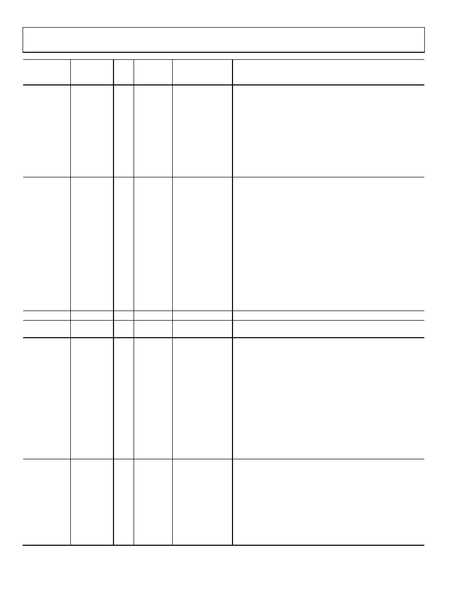
AD9882A
Rev. 0 | Page 24 of 40
Hexadecimal
Address
Read and
Write or
Read Only
Bit
Default
Value
Register Name
Function
4
***0 ****
Active Hsync
Override
0 = No override.
1 = User overrides, analog Hsync set by 0x10, Bit 3.
3
**** 0***
Active Hsync
Select
0 = Analog Hsync from the Hsync input pin.
1 = Analog Hsync from SOG. This bit is used if Register 0x10, Bit 4
is set to 1 or if both syncs are active.
2
**** *0**
Output Vsync
Polarity
0 = Invert.
1 = Not inverted.
1
**** **0*
Active Vsync
Override
0 = No override.
1 = User overrides, analog Vsync set by 0x10, Bit 0.
0
**** ***0
Active Vsync
Select
0 = Analog Vsync from the Vsync input pin.
1 = Analog Vsync from sync separator.
0x11
R/W
7
0*** ****
Clamp Function
0 = Clamping with internal clamp.
1 = Clamping disabled.
6
*0** ****
Red Clamp Select
0 = Clamp to ground.
1 = Clamp to midscale for red channel.
5
**0* ****
Green Clamp
Select
0 = Clamp to ground.
1 = Clamp to midscale for green channel.
4
***0 ****
Blue Clamp Select
0 = Clamp to ground.
1 = Clamp to midscale for blue channel.
3
**** 1***
Coast Select
0 = Disabled coast.
1 = Coasting with internally generated coast signal.
2
**** *0**
Coast Polarity
Override
0 = Coast polarity determined by the chip.
1 = Coast polarity set by 0x11, Bit 1. This bit must be set to 1 to
disable coast.
1
**** **1*
Input Coast
Polarity
0 = Active low coast signal.
1 = Active high coast signal. This bit must be set to 1 to disable
coast.
0x12
R/W
7–0
0000 0000
Precoast
Number of Hsync periods that coast goes active prior to Vsync.
0x13
R/W
7–0
0000 0000
Postcoast
Number of Hsync periods before coast goes inactive following
Vsync.
0x14
R/W
7–6
11** ****
Output Drive
Select
Selects among high, medium, and low output drive strength.
5
**1* ****
Programmable
Bandwidth
0 = Low bandwidth of 10 MHz.
1 = High bandwidth of 300 MHz.
4
***0 ****
DVI Clock Invert
0 = DVI data clock output not inverted.
1 = DVI data clock output inverted.
For digital interface only.
3
**** 0***
DVI PDO Three-
State
0 = Normal outputs.
1 = High impedance outputs.
2
**** *0**
HDCP Address
Address Bit 0 = 0 for HDCP slave port.
Address Bit 1 = 1 for HDCP slave port.
1
**** **1*
Power-Down
0 = Full chip power-down.
0
**** ***0
Enable 4:2:2
0 = 4:4:4 mode.
1 = 4:2:2 mode.
0x15
RO
7
Analog Hsync
Active
0 = Hsync not detected.
1 = Hsync detected.
6
Analog SOG
Active
0 = Sync signal not detected on green channel.
1 = Sync signal detected on green channel.
5
Analog Vsync
Active
0 = Vsync not detected.
1 = Vsync detected.
4
DVI Active
0 = Digital interface clock not detected.
1 = Digital interface clock detected.
3
Active Interface
0 = Analog interface active.
1 = DVI interface active.
相关PDF资料 |
PDF描述 |
|---|---|
| MS27473E16B55PA | CONN PLUG 55POS STRAIGHT W/PINS |
| LTC4305IGN#TR | IC BUFFER BUS 2WR ADDRESS 16SSOP |
| VI-B43-IW-F2 | CONVERTER MOD DC/DC 24V 100W |
| AD9983AKCPZ-170 | IC INTRFACE 8BIT 170MSPS 64LFCSP |
| VI-B42-IX-F4 | CONVERTER MOD DC/DC 15V 75W |
相关代理商/技术参数 |
参数描述 |
|---|---|
| AD9882KSTZ-140 | 功能描述:IC INTERFACE/DVI 100MHZ 100LQFP RoHS:是 类别:集成电路 (IC) >> 接口 - 专用 系列:- 特色产品:NXP - I2C Interface 标准包装:1 系列:- 应用:2 通道 I²C 多路复用器 接口:I²C,SM 总线 电源电压:2.3 V ~ 5.5 V 封装/外壳:16-TSSOP(0.173",4.40mm 宽) 供应商设备封装:16-TSSOP 包装:剪切带 (CT) 安装类型:表面贴装 产品目录页面:825 (CN2011-ZH PDF) 其它名称:568-1854-1 |
| AD9883 | 制造商:AD 制造商全称:Analog Devices 功能描述:110 MSPS Analog Interface for Flat Panel Displays |
| AD9883/PCB | 制造商:AD 制造商全称:Analog Devices 功能描述:110 MSPS Analog Interface for Flat Panel Displays |
| AD9883A | 制造商:AD 制造商全称:Analog Devices 功能描述:110 MSPS/140 MSPS Analog Interface for Flat Panel Displays |
| AD9883A/PCB | 制造商:Analog Devices 功能描述:110MHZ ANALOG INTERFACE FOR SG |
发布紧急采购,3分钟左右您将得到回复。