- 您现在的位置:买卖IC网 > PDF目录11767 > AD9882KSTZ-100 (Analog Devices Inc)IC INTERFACE/DVI 100MHZ 100LQFP PDF资料下载
参数资料
| 型号: | AD9882KSTZ-100 |
| 厂商: | Analog Devices Inc |
| 文件页数: | 8/40页 |
| 文件大小: | 0K |
| 描述: | IC INTERFACE/DVI 100MHZ 100LQFP |
| 标准包装: | 1 |
| 应用: | 视频 |
| 接口: | 模拟,DVI |
| 电源电压: | 3.15 V ~ 3.45 V |
| 封装/外壳: | 100-LQFP |
| 供应商设备封装: | 100-LQFP(14x14) |
| 包装: | 管件 |
| 安装类型: | 表面贴装 |
第1页第2页第3页第4页第5页第6页第7页当前第8页第9页第10页第11页第12页第13页第14页第15页第16页第17页第18页第19页第20页第21页第22页第23页第24页第25页第26页第27页第28页第29页第30页第31页第32页第33页第34页第35页第36页第37页第38页第39页第40页
AD9882A
Rev. 0 | Page 16 of 40
Four programmable registers are provided to optimize the
performance of the PLL. These registers are
1.
The 12-bit divisor register (Registers 0x01 and 0x02). The
input Hsync frequencies range from 15 kHz to 110 kHz.
The PLL multiplies the frequency of the Hsync signal,
producing pixel clock frequencies in the range of 12 MHz
to 140 MHz. The divisor register controls the exact
multiplication factor. This register can be set to any value
between 221 and 4095. The divide ratio that is actually
used is the programmed divide ratio plus one.
2.
The 2-bit VCO range register (Register 0x03, Bits 6 and 7).
To improve the noise performance of the AD9882A, the
VCO operating frequency range is divided into three
overlapping regions. The VCO range register sets this
operating range. The frequency ranges for the lowest and
highest regions are shown in Table 8.
3.
The 3-bit charge pump current register (Register 0x03,
Bits 3 to 5). This register allows the current that drives the
low-pass loop filter to be varied. The possible current
values are listed in Table 9.
4.
The 5-bit Phase Adjust Register (Register 0x04, Bits 3 to 7).
The phase of the generated sampling clock can be shifted
to locate an optimum sampling point within a clock cycle.
The phase adjust register provides 32 phase-shift steps of
11.25° each. The Hsync signal with an identical phase shift
is available through the HSOUT pin.
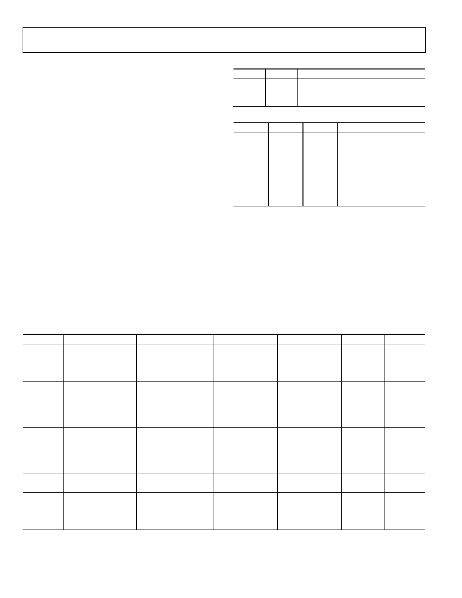
Table 8. VCO Frequency Ranges
PV1
PV0
Pixel Clock Range (MHz)
0
12–41
0
1
41–82
1
0
82–140
Table 9. Charge Pump Current/Control Bits
Ip2
Ip1
Ip0
Current (A)
0
50
0
1
100
0
1
0
150
0
1
250
1
0
350
1
0
1
500
1
0
750
1
1500
The coast function allows the PLL to continue to run at the
same frequency, in the absence of the incoming Hsync signal or
during disturbances in Hsync (such as equalization pulses).
This can be used during the vertical sync period, or any other
time that the Hsync signal is unavailable. Also, the polarity of
the Hsync signal can be set through the Hsync polarity bit
(Register 0x10, Bit 6). If not using automatic polarity detection,
the Hsync polarity bit should be set to match the polarity of the
Hsync input signal.
Table 10. Recommended VCO Range and Charge Pump Current Settings for Standard Display Formats
Standard
Refresh Resolution
Horizontal Rate (Hz)
Frequency (kHz)
Pixel Rate (MHz)
VCORNGE
CURRENT
VGA
640 × 480
60
31.500
25.175
00
101
72
37.700
31.500
00
101
75
37.500
31.500
00
101
85
43.300
36.000
00
110
SVGA
800 × 600
56
35.100
36.000
00
101
60
37.900
40.000
00
110
72
48.100
50.000
01
101
75
46.900
49.500
01
101
85
53.700
56.250
01
101
XGA
1024 × 768
60
48.400
65.000
01
101
70
56.500
75.000
01
110
75
60.000
78.750
01
110
80
64.000
85.500
10
101
85
68.300
94.500
10
101
SXGA
1280 × 1024
60
64.000
108.000
10
101
75
80.000
135.000
10
110
TV Modes
480i
60
15.750
13.500
00
001
480p
60
31.470
27.000
00
100
720p
60
45.000
74.500
01
101
1080i
60
33.750
74.500
01
101
相关PDF资料 |
PDF描述 |
|---|---|
| MS27473E16B55PA | CONN PLUG 55POS STRAIGHT W/PINS |
| LTC4305IGN#TR | IC BUFFER BUS 2WR ADDRESS 16SSOP |
| VI-B43-IW-F2 | CONVERTER MOD DC/DC 24V 100W |
| AD9983AKCPZ-170 | IC INTRFACE 8BIT 170MSPS 64LFCSP |
| VI-B42-IX-F4 | CONVERTER MOD DC/DC 15V 75W |
相关代理商/技术参数 |
参数描述 |
|---|---|
| AD9882KSTZ-140 | 功能描述:IC INTERFACE/DVI 100MHZ 100LQFP RoHS:是 类别:集成电路 (IC) >> 接口 - 专用 系列:- 特色产品:NXP - I2C Interface 标准包装:1 系列:- 应用:2 通道 I²C 多路复用器 接口:I²C,SM 总线 电源电压:2.3 V ~ 5.5 V 封装/外壳:16-TSSOP(0.173",4.40mm 宽) 供应商设备封装:16-TSSOP 包装:剪切带 (CT) 安装类型:表面贴装 产品目录页面:825 (CN2011-ZH PDF) 其它名称:568-1854-1 |
| AD9883 | 制造商:AD 制造商全称:Analog Devices 功能描述:110 MSPS Analog Interface for Flat Panel Displays |
| AD9883/PCB | 制造商:AD 制造商全称:Analog Devices 功能描述:110 MSPS Analog Interface for Flat Panel Displays |
| AD9883A | 制造商:AD 制造商全称:Analog Devices 功能描述:110 MSPS/140 MSPS Analog Interface for Flat Panel Displays |
| AD9883A/PCB | 制造商:Analog Devices 功能描述:110MHZ ANALOG INTERFACE FOR SG |
发布紧急采购,3分钟左右您将得到回复。