- 您现在的位置:买卖IC网 > PDF目录11767 > AD9882KSTZ-100 (Analog Devices Inc)IC INTERFACE/DVI 100MHZ 100LQFP PDF资料下载
参数资料
| 型号: | AD9882KSTZ-100 |
| 厂商: | Analog Devices Inc |
| 文件页数: | 7/40页 |
| 文件大小: | 0K |
| 描述: | IC INTERFACE/DVI 100MHZ 100LQFP |
| 标准包装: | 1 |
| 应用: | 视频 |
| 接口: | 模拟,DVI |
| 电源电压: | 3.15 V ~ 3.45 V |
| 封装/外壳: | 100-LQFP |
| 供应商设备封装: | 100-LQFP(14x14) |
| 包装: | 管件 |
| 安装类型: | 表面贴装 |
第1页第2页第3页第4页第5页第6页当前第7页第8页第9页第10页第11页第12页第13页第14页第15页第16页第17页第18页第19页第20页第21页第22页第23页第24页第25页第26页第27页第28页第29页第30页第31页第32页第33页第34页第35页第36页第37页第38页第39页第40页
AD9882A
Rev. 0 | Page 15 of 40
SYNC-ON-GREEN (SOG)
The sync-on-green input operates in two steps. First, it sets a
baseline clamp level off of the incoming video signal with a
negative peak detector. Second, it sets the sync trigger level
(nominally 150 mV above the negative peak). The exact trigger
level is variable and can be programmed via Register 0x0F,
Bits 7 to 3. The sync-on-green input must be ac-coupled to the
green analog input through its own capacitor as shown in
Figure 5. The value of the capacitor must be 1 nF ±20%. If sync-
on-green is not used, this connection is not required and
SOGIN should be left unconnected. Note that the sync-on-
green signal is always negative polarity. See the Sync Processing
Engine section for further information.
05123-005
GAIN
SOGIN
1nF
RAIN
47nF
BAIN
47nF
Figure 5. Typical Clamp Configuration
CLOCK GENERATION
A phase-locked loop (PLL) is employed to generate the pixel
clock. The Hsync input provides a reference frequency for the
PLL. A voltage controlled oscillator (VCO) generates a much
higher pixel clock frequency. This pixel clock is divided by the
PLL divide value (Registers 0x01 and 0x02) and phase com-
pared with the Hsync input. Any error is used to shift the VCO
frequency and maintain lock between the two signals.
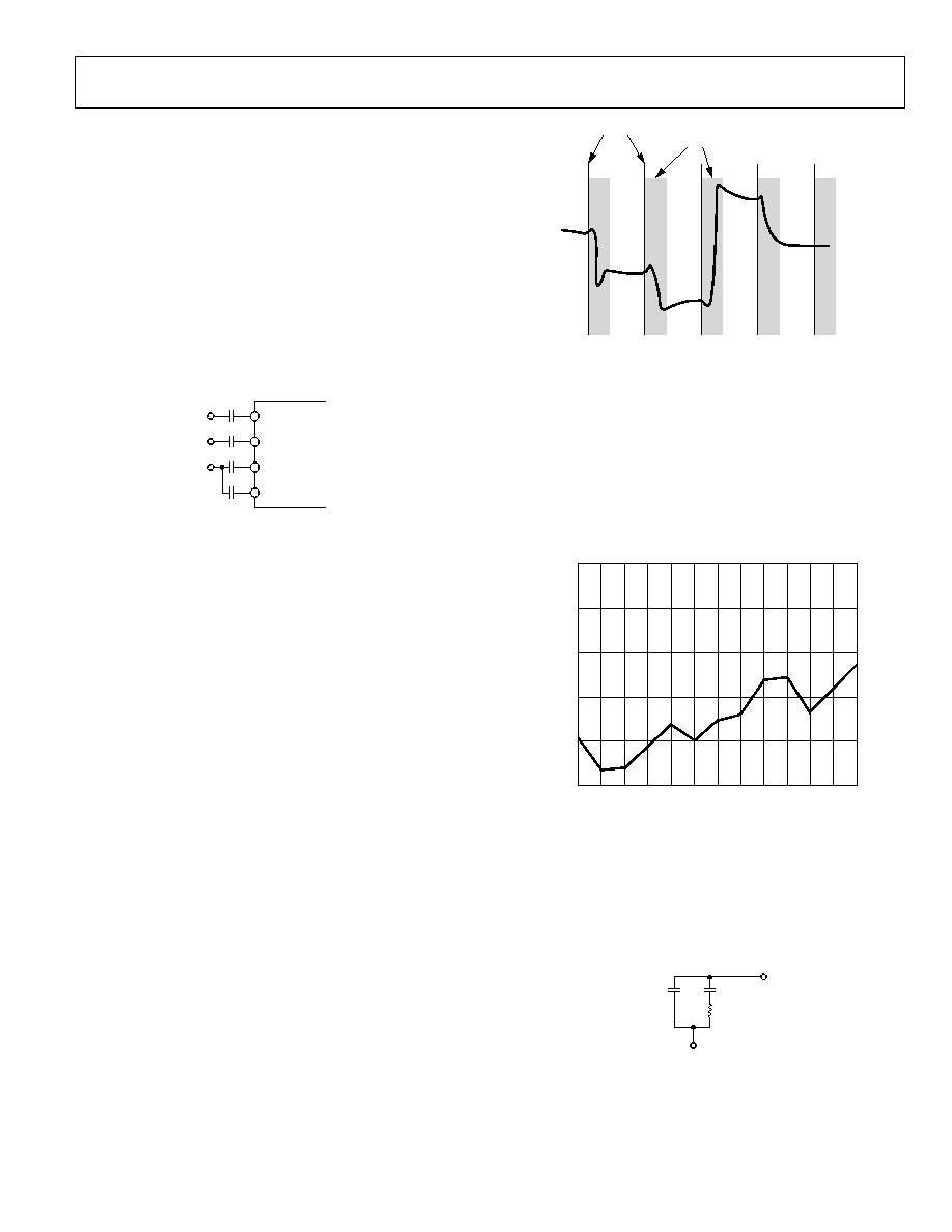
The stability of this clock is a very important element in provid-
ing the clearest and most stable image. During each pixel time,
there is a period during which the signal is slewing from the old
pixel amplitude and settling at its new value. Then there is a
time when the input voltage is stable, before the signal must
slew to a new value (Figure 6). The ratio of the slewing time to
the stable time is a function of the bandwidth of the graphics
DAC and the bandwidth of the transmission system (cable and
termination). It is also a function of the overall pixel rate.
Clearly, if the dynamic characteristics of the system remain
fixed, then the slewing and settling time is likewise fixed. This
time must be subtracted from the total pixel period, leaving the
stable period. At higher pixel frequencies, the total cycle time is
shorter, and the stable pixel time becomes shorter as well.
05123-006
PIXEL CLOCK
INVALID SAMPLE TIMES
Figure 6. Pixel Sampling Times
Any jitter in the clock reduces the precision with which the
sampling time can be determined and must also be subtracted
from the stable pixel time.
Considerable care has been taken in the design of the
AD9882A’s clock generation circuit to minimize jitter. As
indicated in Figure 7, the clock jitter of the AD9882A is less
than 6% of the total pixel time in all operating modes, making
negligible the reduction in the valid sampling time due to jitter.
10
8
6
4
2
0
25.1
31.5
36.0
40.0
50.0
56.2
65.0
75.0
78.7
85.5
94.5 108.0 135.0
05123-007
PIXEL CLOCK FREQUENCY (MHz)
P
IX
E
L
CLO
CK
J
ITTE
R
(p-p)
(%
)
Figure 7. Pixel Clock Jitter vs. Frequency
The PLL characteristics are determined by the loop filter design,
the PLL charge pump current, and the VCO range setting. The
loop filter design is illustrated in Figure 8. Recommended
settings of VCO range and charge pump current for VESA
standard display modes are listed in Table 10.
05123-008
CP
0.0082
F
CZ
0.082
F
RZ
2.74k
FILT
PVD
Figure 8. PLL Loop Filter Detail
相关PDF资料 |
PDF描述 |
|---|---|
| MS27473E16B55PA | CONN PLUG 55POS STRAIGHT W/PINS |
| LTC4305IGN#TR | IC BUFFER BUS 2WR ADDRESS 16SSOP |
| VI-B43-IW-F2 | CONVERTER MOD DC/DC 24V 100W |
| AD9983AKCPZ-170 | IC INTRFACE 8BIT 170MSPS 64LFCSP |
| VI-B42-IX-F4 | CONVERTER MOD DC/DC 15V 75W |
相关代理商/技术参数 |
参数描述 |
|---|---|
| AD9882KSTZ-140 | 功能描述:IC INTERFACE/DVI 100MHZ 100LQFP RoHS:是 类别:集成电路 (IC) >> 接口 - 专用 系列:- 特色产品:NXP - I2C Interface 标准包装:1 系列:- 应用:2 通道 I²C 多路复用器 接口:I²C,SM 总线 电源电压:2.3 V ~ 5.5 V 封装/外壳:16-TSSOP(0.173",4.40mm 宽) 供应商设备封装:16-TSSOP 包装:剪切带 (CT) 安装类型:表面贴装 产品目录页面:825 (CN2011-ZH PDF) 其它名称:568-1854-1 |
| AD9883 | 制造商:AD 制造商全称:Analog Devices 功能描述:110 MSPS Analog Interface for Flat Panel Displays |
| AD9883/PCB | 制造商:AD 制造商全称:Analog Devices 功能描述:110 MSPS Analog Interface for Flat Panel Displays |
| AD9883A | 制造商:AD 制造商全称:Analog Devices 功能描述:110 MSPS/140 MSPS Analog Interface for Flat Panel Displays |
| AD9883A/PCB | 制造商:Analog Devices 功能描述:110MHZ ANALOG INTERFACE FOR SG |
发布紧急采购,3分钟左右您将得到回复。