- 您现在的位置:买卖IC网 > PDF目录11767 > AD9882KSTZ-100 (Analog Devices Inc)IC INTERFACE/DVI 100MHZ 100LQFP PDF资料下载
参数资料
| 型号: | AD9882KSTZ-100 |
| 厂商: | Analog Devices Inc |
| 文件页数: | 39/40页 |
| 文件大小: | 0K |
| 描述: | IC INTERFACE/DVI 100MHZ 100LQFP |
| 标准包装: | 1 |
| 应用: | 视频 |
| 接口: | 模拟,DVI |
| 电源电压: | 3.15 V ~ 3.45 V |
| 封装/外壳: | 100-LQFP |
| 供应商设备封装: | 100-LQFP(14x14) |
| 包装: | 管件 |
| 安装类型: | 表面贴装 |
第1页第2页第3页第4页第5页第6页第7页第8页第9页第10页第11页第12页第13页第14页第15页第16页第17页第18页第19页第20页第21页第22页第23页第24页第25页第26页第27页第28页第29页第30页第31页第32页第33页第34页第35页第36页第37页第38页当前第39页第40页
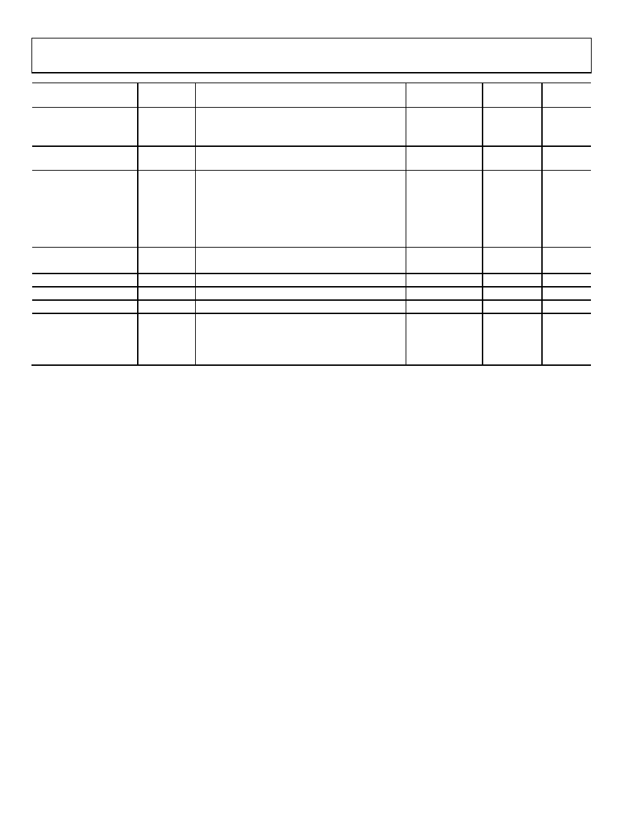
AD9882A
Rev. 0 | Page 8 of 40
Pin Type
Mnemonic
Function
Value
Pin
Number
Interface
Data Outputs
RED [7:0]
Outputs of Converter Red, Bit 7 is the MSB
3.3 V CMOS
92–99
Both
GREEN [7:0]
Outputs of Converter Green, Bit 7 is the MSB
3.3 V CMOS
2–9
Both
BLUE [7:0]
Outputs of Converter Bue, Bit 7 is the MSB
3.3 V CMOS
12–19
Both
Data Clock Output
DATACK
Data Output Clock for the Analog and Digital
Interface
3.3 V CMOS
85
Both
RX0+
Digital Input Channel 0 True
33
Digital
Digital Video Data
Inputs
RX0–
Digital Input Channel 0 Complement
32
Digital
RX1+
Digital Input Channel 1 True
36
Digital
RX1–
Digital Input Channel 1 Complement
35
Digital
RX2+
Digital Input Channel 2 True
39
Digital
RX2–
Digital Input Channel 2 Complement
38
Digital
RXC+
Digital Data Clock True
41
Digital
Digital Video Clock
Inputs
RXC–
Digital Data Clock Complement
42
Digital
Data Enable
DE
Data Enable
3.3 V CMOS
86
Digital
Control Bits
CTL [0:3]
Decoded Control Bits
3.3 V CMOS
22–25
Digital
RTERM
RTERM
Sets Internal Termination Resistance
28
Digital
HDCP
DDCSCL
HDCP Slave Serial Port Data Clock
3.3 V CMOS
53
Digital
DDCSDA
HDCP Slave Serial Port Data I/O
3.3 V CMOS
54
Digital
MCL
HDCP Master Serial Port Data Clock
3.3 V CMOS
81
Digital
MDA
HDCP Master Serial Port Data I/O
3.3 V CMOS
82
Digital
PIN DESCRIPTIONS OF SHARED PINS BETWEEN
ANALOG AND DIGITAL INTERFACES
HSOUT—Horizontal Sync Output
A reconstructed and phase-aligned version of the video Hsync.
The polarity of this output can be controlled via a serial bus bit.
In analog interface mode, the placement and duration are
variable. In digital interface mode, the placement and duration
are set by the graphics transmitter.
VSOUT—Vertical Sync Output
The separated Vsync from a composite signal or a direct pass-
through of the Vsync input. The polarity of this output can be
controlled via a serial bus bit. The placement and duration in all
modes is set by the graphics transmitter.
SERIAL PORT (2-WIRE)
SDA—Serial Port Data I/O
SCL—Serial Port Data Clock
A0—Serial Port Address Input
For a full description of the 2-wire serial register, refer to the
DATA OUTPUTS
RED—Data Output, Red Channel
GREEN—Data Output, Green Channel
BLUE—Data Output, Blue Channel
The main data outputs. Bit 7 is the MSB. These outputs are
shared between the two interfaces and behave in accordance
with the active interface. Refer to the Analog Interface and
Digital Interface sections.
DATACK—Data Output Clock
Just like the data outputs, the data clock output is shared
between the two interfaces. It behaves differently depending on
which interface is active. Refer to the DATACK—Data Output
section to determine how this pin behaves. .
相关PDF资料 |
PDF描述 |
|---|---|
| MS27473E16B55PA | CONN PLUG 55POS STRAIGHT W/PINS |
| LTC4305IGN#TR | IC BUFFER BUS 2WR ADDRESS 16SSOP |
| VI-B43-IW-F2 | CONVERTER MOD DC/DC 24V 100W |
| AD9983AKCPZ-170 | IC INTRFACE 8BIT 170MSPS 64LFCSP |
| VI-B42-IX-F4 | CONVERTER MOD DC/DC 15V 75W |
相关代理商/技术参数 |
参数描述 |
|---|---|
| AD9882KSTZ-140 | 功能描述:IC INTERFACE/DVI 100MHZ 100LQFP RoHS:是 类别:集成电路 (IC) >> 接口 - 专用 系列:- 特色产品:NXP - I2C Interface 标准包装:1 系列:- 应用:2 通道 I²C 多路复用器 接口:I²C,SM 总线 电源电压:2.3 V ~ 5.5 V 封装/外壳:16-TSSOP(0.173",4.40mm 宽) 供应商设备封装:16-TSSOP 包装:剪切带 (CT) 安装类型:表面贴装 产品目录页面:825 (CN2011-ZH PDF) 其它名称:568-1854-1 |
| AD9883 | 制造商:AD 制造商全称:Analog Devices 功能描述:110 MSPS Analog Interface for Flat Panel Displays |
| AD9883/PCB | 制造商:AD 制造商全称:Analog Devices 功能描述:110 MSPS Analog Interface for Flat Panel Displays |
| AD9883A | 制造商:AD 制造商全称:Analog Devices 功能描述:110 MSPS/140 MSPS Analog Interface for Flat Panel Displays |
| AD9883A/PCB | 制造商:Analog Devices 功能描述:110MHZ ANALOG INTERFACE FOR SG |
发布紧急采购,3分钟左右您将得到回复。