- 您现在的位置:买卖IC网 > PDF目录1894 > AD9887AKSZ-140 (Analog Devices Inc)IC INTRFACE ANALOG/DVI 160-MQFP PDF资料下载
参数资料
| 型号: | AD9887AKSZ-140 |
| 厂商: | Analog Devices Inc |
| 文件页数: | 20/52页 |
| 文件大小: | 0K |
| 描述: | IC INTRFACE ANALOG/DVI 160-MQFP |
| 标准包装: | 24 |
| 应用: | 图形卡,VGA 接口 |
| 接口: | 模拟和数字 |
| 电源电压: | 3.15 V ~ 3.45 V |
| 封装/外壳: | 160-BQFP |
| 供应商设备封装: | 160-MQFP(28x28) |
| 包装: | 托盘 |
| 安装类型: | 表面贴装 |
| 产品目录页面: | 788 (CN2011-ZH PDF) |
第1页第2页第3页第4页第5页第6页第7页第8页第9页第10页第11页第12页第13页第14页第15页第16页第17页第18页第19页当前第20页第21页第22页第23页第24页第25页第26页第27页第28页第29页第30页第31页第32页第33页第34页第35页第36页第37页第38页第39页第40页第41页第42页第43页第44页第45页第46页第47页第48页第49页第50页第51页第52页
AD9887A
Rev. B | Page 27 of 52
THEORY OF OPERATION—INTERFACE DETECTION
ACTIVE INTERFACE DETECTION AND SELECTION
For interface detection in the AD9887A, the system should
determine the correct interface and set the chip appropriately
through the serial bus. An external circuit should be used to
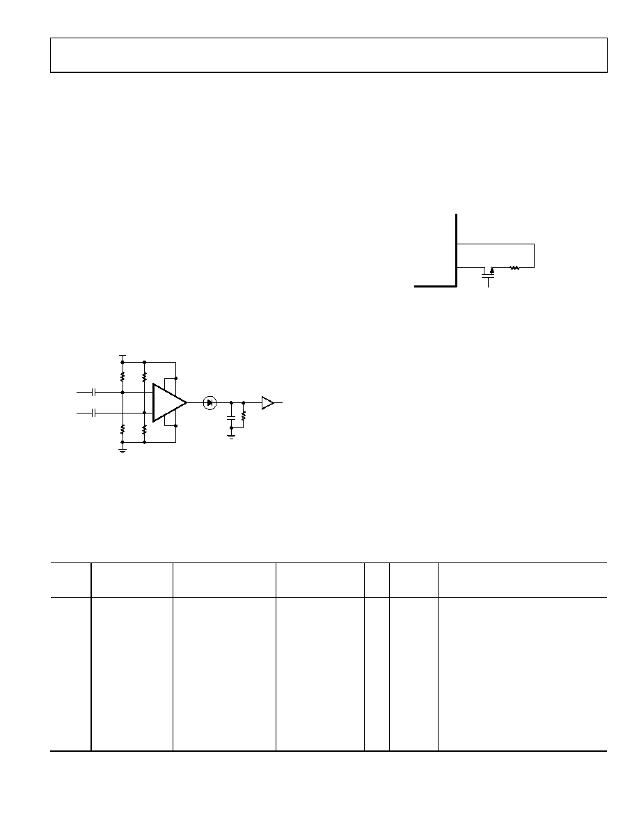
determine if the digital interface is active. A typical schematic
for this detection function is shown in Figure 28.
It is recommended that the system implement the interface
selection criteria, as described in Table 8. Because the digital
interface clock detect bit (0x11[4]) has been unreliable in some
applications, it is recommended that the active interface override
bit (0x12[7]) be set to 1. This allows the system to select the
interface through the serial bus register active interface select
(AIS) bit (0x12[6]). This selection should be based on the analog
interface detect obtained by OR’ing Bit 7, Bit 6, and Bit 5 of
Register 0x11 and on the digital interface detect obtained through
the external circuitry shown in Figure 28. When both interfaces
are active, priority must be determined by the system and the
appropriate interface must be selected via the AIS bit.
+
–
9
10
1
2
5
6
8
10k
11k
10k
0.1F
CLK+
CLK–
1.0F
10k
CLK
ACTIVE
3.3V
1 = DVI CLOCK ACTIVE
0 = DVI CLOCK NOT ACTIVE
HIGH SPEED
COMPARATOR
LT1715
02
83
8-
0
43
Figure 28. External Digital Interface Clock Detect Circuit
HOT-PLUG DETECT
In some HDCP-enabled applications it may be desirable to be
able to switch between the analog and DVI interfaces without
having an DVI plug/unplug event. In these applications, the circuit
in Figure 29 should be used for the hot-plug detect connection.
The FET switch should be controlled by the system-level software
to force an HPD event whenever the selected interface is switched
from the analog input to the DVI input.
HPD
+5V
14
15
HPD CONTROL BIT
02
83
8-
0
46
1k
Figure 29. Manual Hot-Plug Detect
POWER MANAGEMENT
The AD9887A is a dual-interface device with shared outputs.
Because only one interface can be used at a time, the unused
interface should be powered down. When the analog interface is
being used, most of the digital interface circuitry can be powered
down and vice versa. This helps to minimize the total power
dissipation of the AD9887A. In addition, if neither interface has
activity on it, both interfaces should be powered down.
The correct power-down state is set by selecting an interface to
be active through the serial bus when either or both interfaces
are active, and by setting the power-down register bit (0x12[0])
to 0 when neither interface has activity on it. In a given power
mode, not all circuitry in the inactive interface is powered down
completely. When the digital interface is active, Hsync detect
circuitry is not powered down. SOG, outputs, and the band gap
reference are powered up if either interface is active. The serial
bus stays active even if the entire chip is powered down.
Table 8. Interface Selection and Power-Down Controls
Power-
Down
Active Interface
Override
(0x12[7])
Analog Interface
Detect (0x11[7],
0x11[6], or 0x11[5])
Digital Interface
Detect (from
External Circuit)
AIS
Active
Interface
Description
1
X
0
Analog
Force the analog interface active.
1
X
1
Digital
Force the digital interface active.
0
X
0
X
None
Neither interface is detected. Both
interfaces are powered down and
the SCDT pin is set to Logic 0.
1
0
1
Digital
The digital interface is detected.
Power down the analog interface.
1
0
Analog
The analog interface is detected.
Power down the digital interface.
1
0
Analog
Both interfaces are detected. The
analog interface has priority.
1
Digital
Both interfaces are detected. The
digital interface has priority.
相关PDF资料 |
PDF描述 |
|---|---|
| AD9888KSZ-170 | IC ANALOG INTRFC 170MSPS 128MQFP |
| AD9895KBCZRL | IC CCD SIGNAL PROC/GEN 64-CSPBGA |
| AD9910BSVZ-REEL | IC DDS 1GSPS 14BIT PAR 100TQFP |
| AD9911BCPZ-REEL7 | IC DDS 500MSPS DAC 10BIT 56LFCSP |
| AD9912ABCPZ | IC DDS 1GSPS DAC 14BIT 64LFCSP |
相关代理商/技术参数 |
参数描述 |
|---|---|
| AD9887AKSZ-1401 | 制造商:AD 制造商全称:Analog Devices 功能描述:Dual Interface for Flat Panel Display |
| AD9887AKSZ-170 | 功能描述:IC INTRFACE ANALOG/DVI 160-MQFP RoHS:是 类别:集成电路 (IC) >> 接口 - 专用 系列:- 特色产品:NXP - I2C Interface 标准包装:1 系列:- 应用:2 通道 I²C 多路复用器 接口:I²C,SM 总线 电源电压:2.3 V ~ 5.5 V 封装/外壳:16-TSSOP(0.173",4.40mm 宽) 供应商设备封装:16-TSSOP 包装:剪切带 (CT) 安装类型:表面贴装 产品目录页面:825 (CN2011-ZH PDF) 其它名称:568-1854-1 |
| AD9887AKSZ-170 | 制造商:Analog Devices 功能描述:IC DUAL DISPLAY INTERFACE |
| AD9887AKSZ-1701 | 制造商:AD 制造商全称:Analog Devices 功能描述:Dual Interface for Flat Panel Display |
| AD9887APCB | 制造商:AD 制造商全称:Analog Devices 功能描述:Dual Interface for Flat Panel Displays |
发布紧急采购,3分钟左右您将得到回复。