- 您现在的位置:买卖IC网 > PDF目录19504 > ADSP-21363KSWZ-1AA (Analog Devices Inc)IC DSP 32BIT 333MHZ EPAD 144LQFP PDF资料下载
参数资料
| 型号: | ADSP-21363KSWZ-1AA |
| 厂商: | Analog Devices Inc |
| 文件页数: | 12/60页 |
| 文件大小: | 0K |
| 描述: | IC DSP 32BIT 333MHZ EPAD 144LQFP |
| 产品培训模块: | SHARC Processor Overview |
| 标准包装: | 1 |
| 系列: | SHARC® |
| 类型: | 浮点 |
| 接口: | DAI,SPI |
| 时钟速率: | 333MHz |
| 非易失内存: | ROM(512 kB) |
| 芯片上RAM: | 384kB |
| 电压 - 输入/输出: | 3.30V |
| 电压 - 核心: | 1.20V |
| 工作温度: | 0°C ~ 70°C |
| 安装类型: | 表面贴装 |
| 封装/外壳: | 144-LQFP 裸露焊盘 |
| 供应商设备封装: | 144-LQFP(20x20) |
| 包装: | 托盘 |
第1页第2页第3页第4页第5页第6页第7页第8页第9页第10页第11页当前第12页第13页第14页第15页第16页第17页第18页第19页第20页第21页第22页第23页第24页第25页第26页第27页第28页第29页第30页第31页第32页第33页第34页第35页第36页第37页第38页第39页第40页第41页第42页第43页第44页第45页第46页第47页第48页第49页第50页第51页第52页第53页第54页第55页第56页第57页第58页第59页第60页
�� �
�
�ADSP-21362/ADSP-21363/ADSP-21364/ADSP-21365/ADSP-21366�
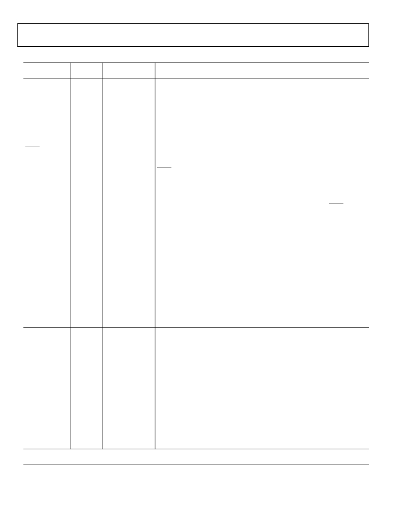
�Table� 6.� Pin� Descriptions� (Continued)�
�State� During� and�
�Pin�
�SPICLK�
�Type�
�I/O�
�(pu)�
�After� Reset�
�Three-state� with�
�pull-up� enabled,�
�driven� high� in� SPI-�
�master� boot� mode�
�Function�
�Serial� Peripheral� Interface� Clock� Signal.� Driven� by� the� master,� this� signal� controls� the�
�rate� at� which� data� is� transferred.� The� master� can� transmit� data� at� a� variety� of� baud� rates.�
�SPICLK� cycles� once� for� each� bit� transmitted.� SPICLK� is� a� gated� clock� active� during� data�
�transfers,� only� for� the� length� of� the� transferred� word.� Slave� devices� ignore� the� serial� clock�
�if� the� slave� select� input� is� driven� inactive� (high).� SPICLK� is� used� to� shift� out� and� shift� in�
�the� data� driven� on� the� MISO� and� MOSI� lines.� The� data� is� always� shifted� out� on� one� clock�
�edge� and� sampled� on� the� opposite� edge� of� the� clock.� Clock� polarity� and� clock� phase�
�relative� to� data� are� programmable� into� the� SPICTL� control� register� and� define� the� transfer�
�format.� SPICLK� has� a� 22.5� k� internal� pull-up� resistor.�
�SPIDS�
�I� Input� only�
�Serial� Peripheral� Interface� Slave� Device� Select.� An� active� low� signal� used� to� select� the�
�processor� as� an� SPI� slave� device.� This� input� signal� behaves� like� a� chip� select,� and� is�
�provided� by� the� master� device� for� the� slave� devices.� In� multimaster� mode� the� processor� ’s�
�SPIDS� signal� can� be� driven� by� a� slave� device� to� signal� to� the� processor� (as� SPI� master)�
�that� an� error� has� occurred,� as� some� other� device� is� also� trying� to� be� the� master� device.� If�
�asserted� low� when� the� device� is� in� master� mode,� it� is� considered� a� multimaster� error.� For�
�a� single-master,� multiple-slave� configuration� where� flag� pins� are� used,� this� pin� must� be�
�tied� or� pulled� high� to� V� DDEXT� on� the� master� device.� For� processor� to� processor� SPI� inter-�
�action,� any� of� the� master� processor� ’s� flag� pins� can� be� used� to� drive� the� SPIDS� signal� on�
�the� SPI� slave� device.�
�MOSI� I/O� (O/D)�
�(pu)�
�MISO� I/O� (O/D)�
�(pu)�
�Three-state� with�
�pull-up� enabled,�
�driven� low� in� SPI-�
�master� boot� mode�
�Three-state� with�
�pull-up� enabled�
�SPI� Master� Out� Slave� In.� If� the� ADSP-2136x� is� configured� as� a� master,� the� MOSI� pin�
�becomes� a� data� transmit� (output)� pin,� transmitting� output� data.� If� the� processor� is�
�configured� as� a� slave,� the� MOSI� pin� becomes� a� data� receive� (input)� pin,� receiving� input�
�data.� In� an� SPI� interconnection,� the� data� is� shifted� out� from� the� MOSI� output� pin� of� the�
�master� and� shifted� into� the� MOSI� input(s)� of� the� slave(s).� MOSI� has� a� 22.5� k� internal� pull-�
�up� resistor.�
�SPI� Master� In� Slave� Out.� If� the� ADSP-2136x� is� configured� as� a� master,� the� MISO� pin�
�becomes� a� data� receive� (input)� pin,� receiving� input� data.� If� the� processor� is� configured�
�as� a� slave,� the� MISO� pin� becomes� a� data� transmit� (output)� pin,� transmitting� output� data.�
�In� an� SPI� interconnection,� the� data� is� shifted� out� from� the� MISO� output� pin� of� the� slave�
�and� shifted� into� the� MISO� input� pin� of� the� master.� MISO� has� a� 22.5� k� internal� pull-up�
�resistor.� MISO� can� be� configured� as� O/D� by� setting� the� OPD� bit� in� the� SPICTL� register.�
�Note:� Only� one� slave� is� allowed� to� transmit� data� at� any� given� time.� To� enable� broadcast�
�transmission� to� multiple� SPI� slaves,� the� processor� ’s� MISO� pin� can� be� disabled� by� setting�
�Bit� 5� (DMISO)� of� the� SPICTL� register� equal� to� 1.�
�CLKIN� I� Input� only�
�Local� Clock� In.� Used� in� conjunction� with� XTAL.� CLKIN� is� the� ADSP-2136x� clock� input.� It�
�configures� the� ADSP-2136x� to� use� either� its� internal� clock� generator� or� an� external� clock�
�source.� Connecting� the� necessary� components� to� CLKIN� and� XTAL� enables� the� internal�
�clock� generator.� Connecting� the� external� clock� to� CLKIN� while� leaving� XTAL� uncon-�
�nected� configures� the� processors� to� use� the� external� clock� source� such� as� an� external�
�clock� oscillator.� The� core� is� clocked� either� by� the� PLL� output� or� this� clock� input� depending�
�on� the� CLK_CFG1–0� pin� settings.� CLKIN� should� not� be� halted,� changed,� or� operated�
�below� the� specified� frequency.�
�XTAL� O� Output� only�
�CLK_CFG1–0� I� Input� only�
�2�
�Crystal� Oscillator� Terminal.� Used� in� conjunction� with� CLKIN� to� drive� an� external� crystal.�
�Core� to� CLKIN� Ratio� Control.� These� pins� set� the� start� up� clock� frequency.� Note� that� the�
�operating� frequency� can� be� changed� by� programming� the� PLL� multiplier� and� divider� in�
�the� PMCTL� register� at� any� time� after� the� core� comes� out� of� reset.� The� allowed� values� are:�
�00� =� 6:1�
�01� =� 32:1�
�10� =� 16:1�
�11� =� reserved.�
�The� following� symbols� appear� in� the� Type� column� of� Table� 6� :� A� =� asynchronous,� G� =� ground,� I� =� input,� O� =� output,� P� =� power� supply,�
�S� =� synchronous,� (� A/D� )� =� active� drive,� (� O/D� )� =� open� drain,� and� T� =� three-state,� (� pd� )� =� pull-down� resistor,� (� pu� )� =� pull-up� resistor.�
�Rev.� J� |�
�Page� 12� of� 60� |�
�July� 2013�
�相关PDF资料 |
PDF描述 |
|---|---|
| ADSP-BF537KBCZ-6AV | IC DSP CTLR 16BIT 182CSPBGA |
| V300A2E160BL | CONVERTER MOD DC/DC 2V 160W |
| ADSP-2191MKSTZ-160 | IC DSP CONTROLLER 16BIT 144LQFP |
| MLP2012S2R2T | INDUCTOR MULTILAYER 2.2UH 0805 |
| 10090098-S254VLF | DSUB STR 25POS SOCKET |
相关代理商/技术参数 |
参数描述 |
|---|---|
| ADSP-21363SBBC-ENG | 制造商:AD 制造商全称:Analog Devices 功能描述:SHARC Processor |
| ADSP-21363SBBCZENG | 制造商:AD 制造商全称:Analog Devices 功能描述:SHARC Processor |
| ADSP-21363SBSQ-ENG | 制造商:AD 制造商全称:Analog Devices 功能描述:SHARC Processor |
| ADSP-21363SBSQZENG | 制造商:AD 制造商全称:Analog Devices 功能描述:SHARC Processor |
| ADSP-21363SCSQ-ENG | 制造商:AD 制造商全称:Analog Devices 功能描述:SHARC Processor |
发布紧急采购,3分钟左右您将得到回复。