- 您现在的位置:买卖IC网 > PDF目录19383 > ADSP-BF561SKBCZ-6V (Analog Devices Inc)IC DSP 32BIT 600MHZ 256CSPBGA PDF资料下载
参数资料
| 型号: | ADSP-BF561SKBCZ-6V |
| 厂商: | Analog Devices Inc |
| 文件页数: | 13/64页 |
| 文件大小: | 0K |
| 描述: | IC DSP 32BIT 600MHZ 256CSPBGA |
| 产品培训模块: | Blackfin® Processor Core Architecture Overview Blackfin® Device Drivers Blackfin® Optimizations for Performance and Power Consumption Blackfin® System Services |
| 标准包装: | 1 |
| 系列: | Blackfin® |
| 类型: | 定点 |
| 接口: | SPI,SSP,UART |
| 时钟速率: | 600MHz |
| 非易失内存: | 外部 |
| 芯片上RAM: | 328kB |
| 电压 - 输入/输出: | 2.50V,3.30V |
| 电压 - 核心: | 1.35V |
| 工作温度: | 0°C ~ 70°C |
| 安装类型: | 表面贴装 |
| 封装/外壳: | 256-LFBGA,CSPBGA |
| 供应商设备封装: | 256-CSPBGA(12x12) |
| 包装: | 托盘 |
| 配用: | ADZS-BFAUDIO-EZEXT-ND - BOARD EVAL AUDIO BLACKFIN ADZS-BF561-EZLITE-ND - BOARD EVAL ADSP-BF561 ADZS-BF561-MMSKIT-ND - KIT STARTER MULTIMEDIA BF561 ADZS-BFAV-EZEXT-ND - BOARD DAUGHT ADSP-BF533,37,61KIT |
第1页第2页第3页第4页第5页第6页第7页第8页第9页第10页第11页第12页当前第13页第14页第15页第16页第17页第18页第19页第20页第21页第22页第23页第24页第25页第26页第27页第28页第29页第30页第31页第32页第33页第34页第35页第36页第37页第38页第39页第40页第41页第42页第43页第44页第45页第46页第47页第48页第49页第50页第51页第52页第53页第54页第55页第56页第57页第58页第59页第60页第61页第62页第63页第64页
�� �
�
�ADSP-BF561 �
�board.� All� internal� and� I/O� power� supplies� should� be� well�
�bypassed� with� bypass� capacitors� placed� as� close� to� the�
�ADSP-BF561� processors� as� possible.�
�For� further� details� on� the� on-chip� voltage� regulator� and� related�
�board� design� guidelines,� see� the� Switching� Regulator� Design�
�Considerations� for� ADSP-BF533� Blackfin� Processors� (EE-228)�
��log.com� )—use� site� search� on� “EE-228”.�
�CLKOUT�
�EN�
�Blackfin�
�TO� PLL� CIRCUITRY�
�700� O�
�CLOCK� SIGNALS�
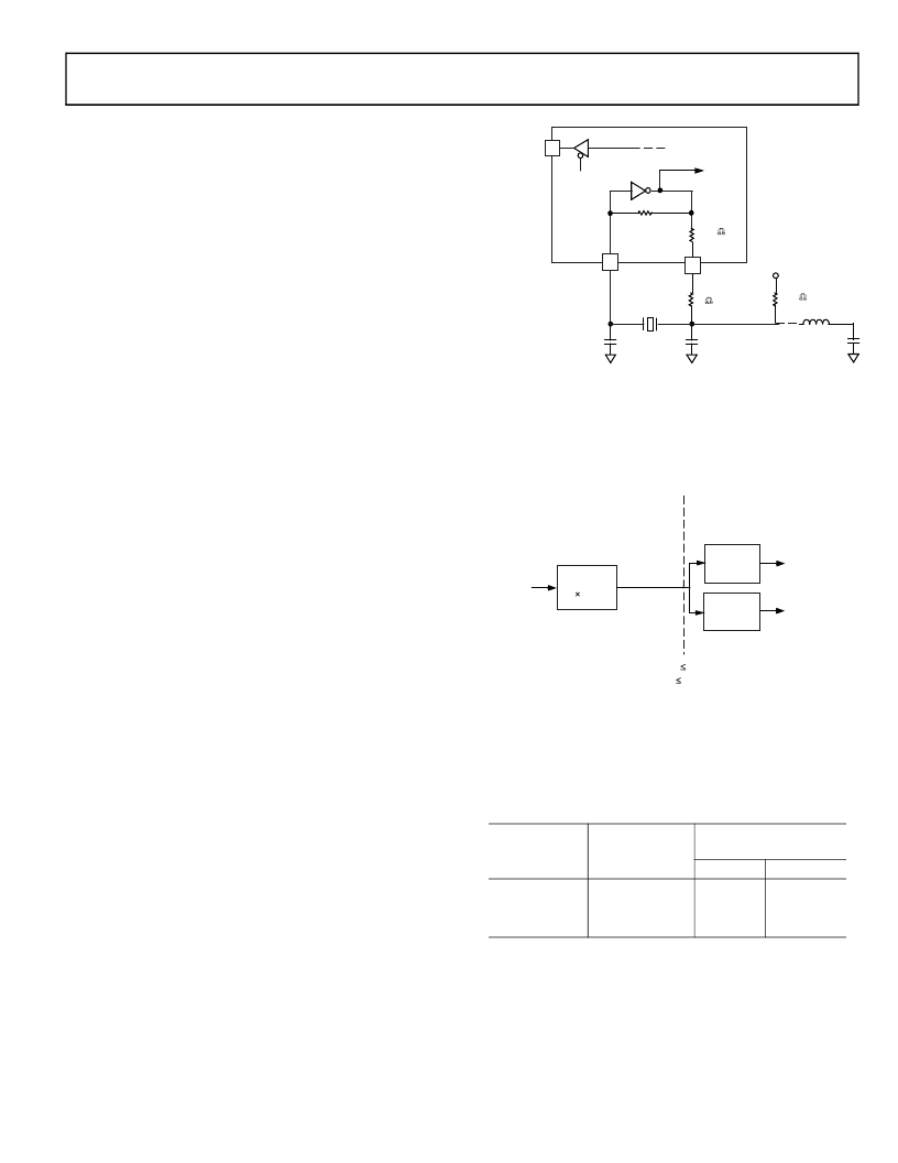
�The� ADSP-BF561� processor� can� be� clocked� by� an� external� crys-�
�tal,� a� sine� wave� input,� or� a� buffered,� shaped� clock� derived� from�
�CLKIN�
�XTAL�
�0� O� *�
�V� DDEXT�
�1M� O�
�an� external� clock� oscillator.�
�If� an� external� clock� is� used,� it� should� be� a� TTL� compatible� signal�
�18pF*�
�18pF*�
�FOR� OVERTONE�
�OPERATION� ONLY�
�and� must� not� be� halted,� changed,� or� operated� below� the� speci-�
�fied� frequency� during� normal� operation.� This� signal� is�
�connected� to� the� processor’s� CLKIN� pin.� When� an� external�
�clock� is� used,� the� XTAL� pin� must� be� left� unconnected.�
�Alternatively,� because� the� ADSP-BF561� processor� includes� an�
�on-chip� oscillator� circuit,� an� external� crystal� may� be� used.� For�
�fundamental� frequency� operation,� use� the� circuit� shown� in�
��NOTE:� VALUES� MARKED� WITH� *� MUST� BE� CUSTOMIZED�
�DEPENDING� ON� THE� CRYSTAL� AND� LAYOUT.� PLEASE�
�ANALYZE� CAREFULLY.�
�Figure� 5.� External� Crystal� Connections�
�processor-grade� crystal� is� connected� across� the� CLKIN� and�
�XTAL� pins.� The� on-chip� resistance� between� CLKIN� and� the�
�XTAL� pin� is� in� the� 500� k� Ω� range.� Further� parallel� resistors� are�
�typically� not� recommended.� The� two� capacitors� and� the� series�
�“FINE”� ADJUSTMENT�
�REQUIRES� PLL� SEQUENCING�
�“COARSE”� ADJUSTMENT�
�ON-THE-FLY�
�resistor� shown� in� Figure� 5� fine� tune� the� phase� and� amplitude� of�
�÷� 1,� 2,� 4,� 8�
�CCLK�
�the� sine� frequency.� The� capacitor� and� resistor� values� shown� in�
��dent� upon� the� crystal� manufacturer’s� load� capacitance�
�CLKIN�
�PLL�
�0.5� u� to� 64� u�
�VCO�
�÷� 1� to� 15�
�SCLK�
�recommendations� and� the� physical� PCB� layout.� The� resistor�
�value� depends� on� the� drive� level� specified� by� the� crystal� manu-�
�Signal� Name�
�Divider� Ratio�
�facturer.� System� designs� should� verify� the� customized� values�
�based� on� careful� investigation� on� multiple� devices� over� the�
�allowed� temperature� range.�
�A� third-overtone� crystal� can� be� used� at� frequencies� above�
�25� MHz.� The� circuit� is� then� modified� to� ensure� crystal� operation�
�only� at� the� third� overtone,� by� adding� a� tuned� inductor� circuit� as�
��As� shown� in� Figure� 6� ,� the� core� clock� (CCLK)� and� system�
�peripheral� clock� (SCLK)� are� derived� from� the� input� clock�
�(CLKIN)� signal.� An� on-chip� PLL� is� capable� of� multiplying� the�
�CLKIN� signal� by� a� user-programmable� 0.5� � to� 64� � multiplica-�
�tion� factor.� The� default� multiplier� is� 10� � ,� but� it� can� be� modified�
�SCLK� d� CCLK�
�SCLK� d� 133� MHz�
�Figure� 6.� Frequency� Modification� Methods�
�into� the� SSEL� fields� define� a� divide� ratio� between� the� PLL� output�
�(VCO)� and� the� system� clock.� SCLK� divider� values� are� 1� through�
�15.� Table� 5� illustrates� typical� system� clock� ratios.�
�Table� 5.� Example� System� Clock� Ratios�
�Example� Frequency�
�Ratios� (MHz)�
�by� a� software� instruction� sequence.� On� the� fly� frequency�
�changes� can� be� effected� by� simply� writing� to� the� PLL_DIV�
�register.�
�All� on-chip� peripherals� are� clocked� by� the� system� clock� (SCLK).�
�The� system� clock� frequency� is� programmable� by� means� of� the�
�SSEL3–0�
�0001�
�0110�
�1010�
�VCO/SCLK�
�1:1�
�6:1�
�10:1�
�VCO�
�100�
�300�
�500�
�SCLK�
�100�
�50�
�50�
�SSEL3–0� bits� of� the� PLL_DIV� register.� The� values� programmed�
�The� maximum� frequency� of� the� system� clock� is� f� SCLK� .� Note� that�
�the� divisor� ratio� must� be� chosen� to� limit� the� system� clock� fre-�
�quency� to� its� maximum� of� f� SCLK� .� The� SSEL� value� can� be� changed�
�dynamically� without� any� PLL� lock� latencies� by� writing� the�
�appropriate� values� to� the� PLL� divisor� register� (PLL_DIV).�
�Rev.� E� |�
�Page� 13� of� 64� |�
�September� 2009�
�相关PDF资料 |
PDF描述 |
|---|---|
| VE-B1T-CV-F3 | CONVERTER MOD DC/DC 6.5V 150W |
| MC7915ACT | IC REG LDO -15V 1A TO220AB |
| MC7912ACT | IC REG LDO -12V 1A TO220AB |
| ADSP-2183KSTZ-210 | IC DSP CONTROLLER 16BIT 128-LQFP |
| ECM12DTBN-S189 | CONN EDGECARD 24POS R/A .156 SLD |
相关代理商/技术参数 |
参数描述 |
|---|---|
| ADSP-BF561SKBCZC70 | 制造商:Analog Devices 功能描述: |
| ADSPBF561SKBCZ-C70 | 制造商:Rochester Electronics LLC 功能描述:- Bulk |
| ADSP-BF561SKBCZENG | 制造商:Analog Devices 功能描述:- Trays |
| ADSP-BF561SKBZ500 | 功能描述:IC DSP 32BIT 500MHZ 297PBGA RoHS:是 类别:集成电路 (IC) >> 嵌入式 - DSP(数字式信号处理器) 系列:Blackfin® 标准包装:2 系列:StarCore 类型:SC140 内核 接口:DSI,以太网,RS-232 时钟速率:400MHz 非易失内存:外部 芯片上RAM:1.436MB 电压 - 输入/输出:3.30V 电压 - 核心:1.20V 工作温度:-40°C ~ 105°C 安装类型:表面贴装 封装/外壳:431-BFBGA,FCBGA 供应商设备封装:431-FCPBGA(20x20) 包装:托盘 |
| ADSP-BF561SKBZ500 | 制造商:Analog Devices 功能描述:Digital Signal Processor IC |
发布紧急采购,3分钟左右您将得到回复。