- 您现在的位置:买卖IC网 > PDF目录19383 > ADSP-BF561SKBCZ-6V (Analog Devices Inc)IC DSP 32BIT 600MHZ 256CSPBGA PDF资料下载
参数资料
| 型号: | ADSP-BF561SKBCZ-6V |
| 厂商: | Analog Devices Inc |
| 文件页数: | 23/64页 |
| 文件大小: | 0K |
| 描述: | IC DSP 32BIT 600MHZ 256CSPBGA |
| 产品培训模块: | Blackfin® Processor Core Architecture Overview Blackfin® Device Drivers Blackfin® Optimizations for Performance and Power Consumption Blackfin® System Services |
| 标准包装: | 1 |
| 系列: | Blackfin® |
| 类型: | 定点 |
| 接口: | SPI,SSP,UART |
| 时钟速率: | 600MHz |
| 非易失内存: | 外部 |
| 芯片上RAM: | 328kB |
| 电压 - 输入/输出: | 2.50V,3.30V |
| 电压 - 核心: | 1.35V |
| 工作温度: | 0°C ~ 70°C |
| 安装类型: | 表面贴装 |
| 封装/外壳: | 256-LFBGA,CSPBGA |
| 供应商设备封装: | 256-CSPBGA(12x12) |
| 包装: | 托盘 |
| 配用: | ADZS-BFAUDIO-EZEXT-ND - BOARD EVAL AUDIO BLACKFIN ADZS-BF561-EZLITE-ND - BOARD EVAL ADSP-BF561 ADZS-BF561-MMSKIT-ND - KIT STARTER MULTIMEDIA BF561 ADZS-BFAV-EZEXT-ND - BOARD DAUGHT ADSP-BF533,37,61KIT |
第1页第2页第3页第4页第5页第6页第7页第8页第9页第10页第11页第12页第13页第14页第15页第16页第17页第18页第19页第20页第21页第22页当前第23页第24页第25页第26页第27页第28页第29页第30页第31页第32页第33页第34页第35页第36页第37页第38页第39页第40页第41页第42页第43页第44页第45页第46页第47页第48页第49页第50页第51页第52页第53页第54页第55页第56页第57页第58页第59页第60页第61页第62页第63页第64页
�� �
�
�ADSP-BF561 �
�TIMING� SPECIFICATIONS�
�Clock� and� Reset� Timing�
���CLKIN� and� clock� multipliers� must� not� result� in� core/system�
�clocks� exceeding� the� maximum� limits� allowed� for� the� processor,�
�including� system� clock� restrictions� related� to� supply� voltage.�
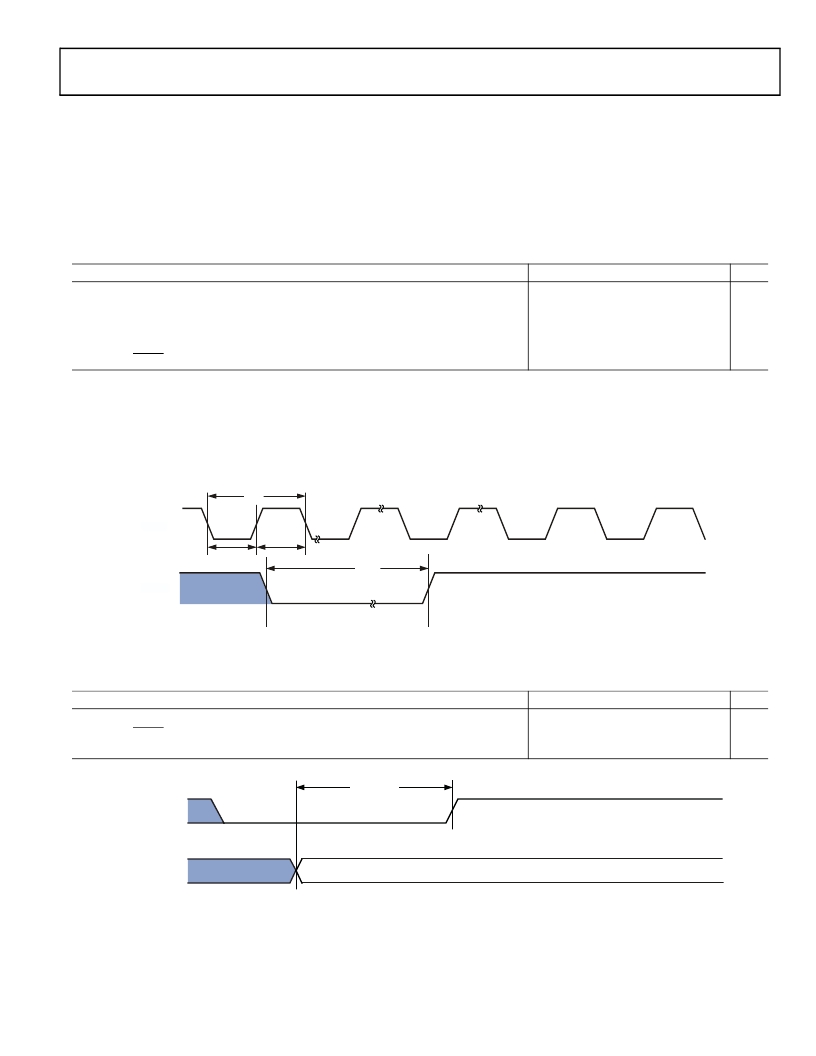
�Table� 16.� Clock� and� Normal� Reset� Timing�
�Parameter�
�Min�
�Max�
�Unit�
�Timing� Requirement� s�
�t� CKIN�
�t� CKINL�
�t� CKINH�
�t� WRST�
�CLKIN� (to� PLL)� Period� 1,� 2,� 3�
�CLKIN� Low� Pulse�
�CLKIN� High� Pulse�
�RESET� Asserted� Pulse� Width� Low� 4�
�25.0�
�10.0�
�10.0�
�11� � t� CKIN�
�100.0�
�ns�
�ns�
�ns�
�ns�
�1�
�2�
�3�
�4�
�If� DF� bit� in� PLL_CTL� register� is� set� t� CLKIN� is� divided� by� two� before� going� to� PLL,� then� the� t� CLKIN� maximum� period� is� 50� ns� and� the� t� CLKIN� minimum� period� is� 12.5� ns.�
�Applies� to� PLL� bypass� mode� and� PLL� nonbypass� mode.�
�Combinations� of� the� CLKIN� frequency� and� the� PLL� clock� multiplier� must� not� exceed� the� allowed� f� VCO� ,� f� CCLK� ,� and� f� SCLK� settings� discussed� in� Table� 9� on� Page� 20� through� Table� 12�
��Applies� after� power-up� sequence� is� complete.� See� Table� 17� and� Figure� 9� for� power-up� reset� timing.�
�t� CKIN�
�CLKIN�
�t� CKINL�
�t� CKINH�
�t� WRST�
�RESET�
�Figure� 8.� Clock� and� Normal� Reset� Timing�
�Table� 17.� Power-Up� Reset� Timing�
�Parameter�
�Min�
�Max�
�Unit�
�Timing� Requirement� s�
�t� RST� _� IN� _� PWR�
�RESET� Deasserted� after� the� V� DDINT� ,� V� DDEXT� ,� and� CLKIN� Pins� are� Stable� and� Within�
�3500� � t� CKIN�
�μ� s�
�Specification�
�t� RST_IN_PWR�
�RESET�
�CLKIN,�
�V� DDINT,� V� DDEXT�
�Figure� 9.� Power-Up� Reset� Timing�
�Rev.� E� |�
�Page� 23� of� 64� |�
�September� 2009�
�相关PDF资料 |
PDF描述 |
|---|---|
| VE-B1T-CV-F3 | CONVERTER MOD DC/DC 6.5V 150W |
| MC7915ACT | IC REG LDO -15V 1A TO220AB |
| MC7912ACT | IC REG LDO -12V 1A TO220AB |
| ADSP-2183KSTZ-210 | IC DSP CONTROLLER 16BIT 128-LQFP |
| ECM12DTBN-S189 | CONN EDGECARD 24POS R/A .156 SLD |
相关代理商/技术参数 |
参数描述 |
|---|---|
| ADSP-BF561SKBCZC70 | 制造商:Analog Devices 功能描述: |
| ADSPBF561SKBCZ-C70 | 制造商:Rochester Electronics LLC 功能描述:- Bulk |
| ADSP-BF561SKBCZENG | 制造商:Analog Devices 功能描述:- Trays |
| ADSP-BF561SKBZ500 | 功能描述:IC DSP 32BIT 500MHZ 297PBGA RoHS:是 类别:集成电路 (IC) >> 嵌入式 - DSP(数字式信号处理器) 系列:Blackfin® 标准包装:2 系列:StarCore 类型:SC140 内核 接口:DSI,以太网,RS-232 时钟速率:400MHz 非易失内存:外部 芯片上RAM:1.436MB 电压 - 输入/输出:3.30V 电压 - 核心:1.20V 工作温度:-40°C ~ 105°C 安装类型:表面贴装 封装/外壳:431-BFBGA,FCBGA 供应商设备封装:431-FCPBGA(20x20) 包装:托盘 |
| ADSP-BF561SKBZ500 | 制造商:Analog Devices 功能描述:Digital Signal Processor IC |
发布紧急采购,3分钟左右您将得到回复。