- 您现在的位置:买卖IC网 > PDF目录294980 > AGL10002-FFGG256 FPGA, 1000000 GATES, 200 MHz, PBGA144 PDF资料下载
参数资料
| 型号: | AGL10002-FFGG256 |
| 元件分类: | FPGA |
| 英文描述: | FPGA, 1000000 GATES, 200 MHz, PBGA144 |
| 封装: | 13 X 13 MM, 1 MM PITCH, ROHS COMPLIANT, FBGA-144 |
| 文件页数: | 167/204页 |
| 文件大小: | 2800K |
| 代理商: | AGL10002-FFGG256 |
第1页第2页第3页第4页第5页第6页第7页第8页第9页第10页第11页第12页第13页第14页第15页第16页第17页第18页第19页第20页第21页第22页第23页第24页第25页第26页第27页第28页第29页第30页第31页第32页第33页第34页第35页第36页第37页第38页第39页第40页第41页第42页第43页第44页第45页第46页第47页第48页第49页第50页第51页第52页第53页第54页第55页第56页第57页第58页第59页第60页第61页第62页第63页第64页第65页第66页第67页第68页第69页第70页第71页第72页第73页第74页第75页第76页第77页第78页第79页第80页第81页第82页第83页第84页第85页第86页第87页第88页第89页第90页第91页第92页第93页第94页第95页第96页第97页第98页第99页第100页第101页第102页第103页第104页第105页第106页第107页第108页第109页第110页第111页第112页第113页第114页第115页第116页第117页第118页第119页第120页第121页第122页第123页第124页第125页第126页第127页第128页第129页第130页第131页第132页第133页第134页第135页第136页第137页第138页第139页第140页第141页第142页第143页第144页第145页第146页第147页第148页第149页第150页第151页第152页第153页第154页第155页第156页第157页第158页第159页第160页第161页第162页第163页第164页第165页第166页当前第167页第168页第169页第170页第171页第172页第173页第174页第175页第176页第177页第178页第179页第180页第181页第182页第183页第184页第185页第186页第187页第188页第189页第190页第191页第192页第193页第194页第195页第196页第197页第198页第199页第200页第201页第202页第203页第204页
IGLOO Low-Power Flash FPGAs with Flash*Freeze Technology
A d v an c ed v0 . 1
2-51
Static (idle) Mode
In Static (idle) mode, none of the clock inputs is
switching, and static power is the only power consumed
by the device. This mode can be achieved by switching
off the incoming clocks to the FPGA benefitting from
reduced power consumption. In addition, I/Os draw only
minimal leakage current. In this mode, embedded SRAM,
I/Os, and registers retain their values so the device can
enter and exit this mode just by switching the clocks on
or off.
If the device embedded PLL is used as the clock source,
Static (idle) mode can easily be entered by pulling LOW
the PLL POWERDOWN pin (active low), which will turn
off the PLL.
Flash*Freeze Mode
IGLOO FPGAs offer an ultra-low static power mode to
reduce power consumption while preserving the state of
the registers and SRAM contents, without switching off
any power supplies, inputs, or input clocks.
Flash*Freeze technology enables the user to switch to
Flash*Freeze mode within 1 s, thus simplifying low-
power design implementation. The Flash*Freeze (FF) pin
(active low) is a dedicated pin used to enter or exit
Flash*Freeze mode directly, or the pin can be routed
internally to the FPGA core to allow the user's logic to
decide if and when it is safe to transition to this mode. If
the FF pin is not used, it can be used as a regular I/O,
benefitting from the inherent low power consumption
of the IGLOO devices.
The FF pin has a built-in glitch filter that ensures spurious
glitches are filtered out to prevent entering or exiting
Flash*Freeze mode accidentally.
There are two ways to use Flash*Freeze mode. In
Flash*Freeze type 1, entering and exiting the mode is
exclusively controlled by the assertion and deassertion of
the FF pin. In Flash*Freeze mode type 2, entering and
exiting the mode is controlled by both the FF pin AND
the user-defined LSICC signal available in the ULSICC
macro.
Refer to Table 2-28 for Flash*Freeze (FF) pin and LSICC
signal assertion and deassertion values.
Flash*Freeze Type 1: Control by
Dedicated Flash*Freeze Pin
The device will enter Flash*Freeze mode 1 s after the
dedicated FF pin is asserted, and returns to normal
operation when the FF pin is deasserted (Figure 2-37). In
this mode, FF pin assertion or deassertion is the only
condition
that
determines
entering
or
exiting
Flash*Freeze mode after 1 s. This mode is implemented
by enabling Flash*Freeze mode (default setting) in the
Compile option of the Actel Designer software.
The FF pin threshold voltages are defined by VCCI and the
supported
single-ended
I/O
standard
in
the
corresponding I/O bank. Figure 2-37 shows the concept
of FF pin control in Flash*Freeze mode type 1.
Figure 2-38 on page 2-52 shows the timing diagram for
entering and exiting Flash*Freeze mode type 1.
Table 2-28 Flash*Freeze Mode Type 1 and Type 2 – Signal
Assertion and Deassertion Values
Signal
Assertion Value
Deassertion
Value
Flash*Freeze (FF) pin
Logic '0'
Logic '1'
LSICC signal
Logic '1'
Logic '0'
Notes:
1. The Flash*Freeze (FF) pin is an active low signal and LSICC is
an active high signal.
2. LSICC signal is used only in Flash*Freeze mode type 2.
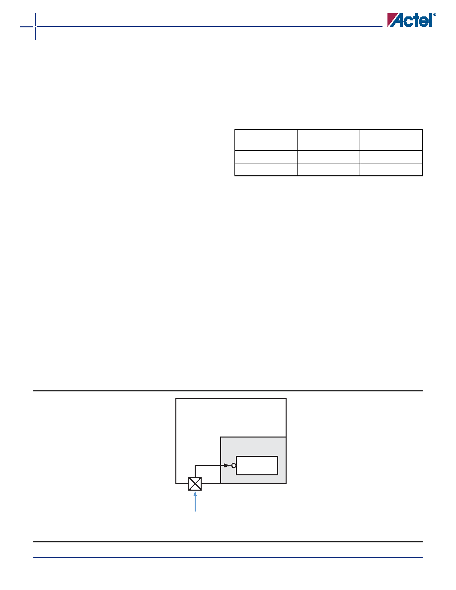
Figure 2-37 IGLOO Flash*Freeze Mode Type 1 – Controlled by the Flash*Freeze Pin
FF Signal
Flash*Freeze
Mode Control
Flash*Freeze (FF) Pin
Flash*Freeze
Technology
Actel IGLOO
FPGA
Flash*Freeze
Mode
相关PDF资料 |
PDF描述 |
|---|---|
| AGL10002-FFGG484I | FPGA, 1000000 GATES, 200 MHz, PBGA484 |
| AGL10002-FFGG484 | FPGA, 1000000 GATES, 200 MHz, PBGA484 |
| AGL10002-FG144I | FPGA, 1000000 GATES, 200 MHz, PBGA144 |
| AGL10002-FG144 | FPGA, 1000000 GATES, 200 MHz, PBGA144 |
| AGL10002-FG256I | FPGA, 1000000 GATES, 200 MHz, PBGA144 |
相关代理商/技术参数 |
参数描述 |
|---|---|
| AGL1000V2-CS144 | 制造商:ACTEL 制造商全称:Actel Corporation 功能描述:IGLOO Low-Power Flash FPGAs with Flash Freeze Technology |
| AGL1000V2-CS144ES | 制造商:ACTEL 制造商全称:Actel Corporation 功能描述:IGLOO Low-Power Flash FPGAs with Flash Freeze Technology |
| AGL1000V2-CS144I | 制造商:ACTEL 制造商全称:Actel Corporation 功能描述:IGLOO Low-Power Flash FPGAs with Flash Freeze Technology |
| AGL1000V2-CS144PP | 制造商:ACTEL 制造商全称:Actel Corporation 功能描述:IGLOO Low-Power Flash FPGAs with Flash Freeze Technology |
| AGL1000V2-CS281 | 功能描述:IC FPGA 1KB FLASH 1M 281-CSP RoHS:否 类别:集成电路 (IC) >> 嵌入式 - FPGA(现场可编程门阵列) 系列:IGLOO 标准包装:40 系列:SX-A LAB/CLB数:6036 逻辑元件/单元数:- RAM 位总计:- 输入/输出数:360 门数:108000 电源电压:2.25 V ~ 5.25 V 安装类型:表面贴装 工作温度:0°C ~ 70°C 封装/外壳:484-BGA 供应商设备封装:484-FPBGA(27X27) |
发布紧急采购,3分钟左右您将得到回复。