- 您现在的位置:买卖IC网 > PDF目录294980 > AGL10002-FFGG256 FPGA, 1000000 GATES, 200 MHz, PBGA144 PDF资料下载
参数资料
| 型号: | AGL10002-FFGG256 |
| 元件分类: | FPGA |
| 英文描述: | FPGA, 1000000 GATES, 200 MHz, PBGA144 |
| 封装: | 13 X 13 MM, 1 MM PITCH, ROHS COMPLIANT, FBGA-144 |
| 文件页数: | 173/204页 |
| 文件大小: | 2800K |
| 代理商: | AGL10002-FFGG256 |
第1页第2页第3页第4页第5页第6页第7页第8页第9页第10页第11页第12页第13页第14页第15页第16页第17页第18页第19页第20页第21页第22页第23页第24页第25页第26页第27页第28页第29页第30页第31页第32页第33页第34页第35页第36页第37页第38页第39页第40页第41页第42页第43页第44页第45页第46页第47页第48页第49页第50页第51页第52页第53页第54页第55页第56页第57页第58页第59页第60页第61页第62页第63页第64页第65页第66页第67页第68页第69页第70页第71页第72页第73页第74页第75页第76页第77页第78页第79页第80页第81页第82页第83页第84页第85页第86页第87页第88页第89页第90页第91页第92页第93页第94页第95页第96页第97页第98页第99页第100页第101页第102页第103页第104页第105页第106页第107页第108页第109页第110页第111页第112页第113页第114页第115页第116页第117页第118页第119页第120页第121页第122页第123页第124页第125页第126页第127页第128页第129页第130页第131页第132页第133页第134页第135页第136页第137页第138页第139页第140页第141页第142页第143页第144页第145页第146页第147页第148页第149页第150页第151页第152页第153页第154页第155页第156页第157页第158页第159页第160页第161页第162页第163页第164页第165页第166页第167页第168页第169页第170页第171页第172页当前第173页第174页第175页第176页第177页第178页第179页第180页第181页第182页第183页第184页第185页第186页第187页第188页第189页第190页第191页第192页第193页第194页第195页第196页第197页第198页第199页第200页第201页第202页第203页第204页
IGLOO Low-Power Flash FPGAs with Flash*Freeze Technology
2- 56
Advanced v0.1
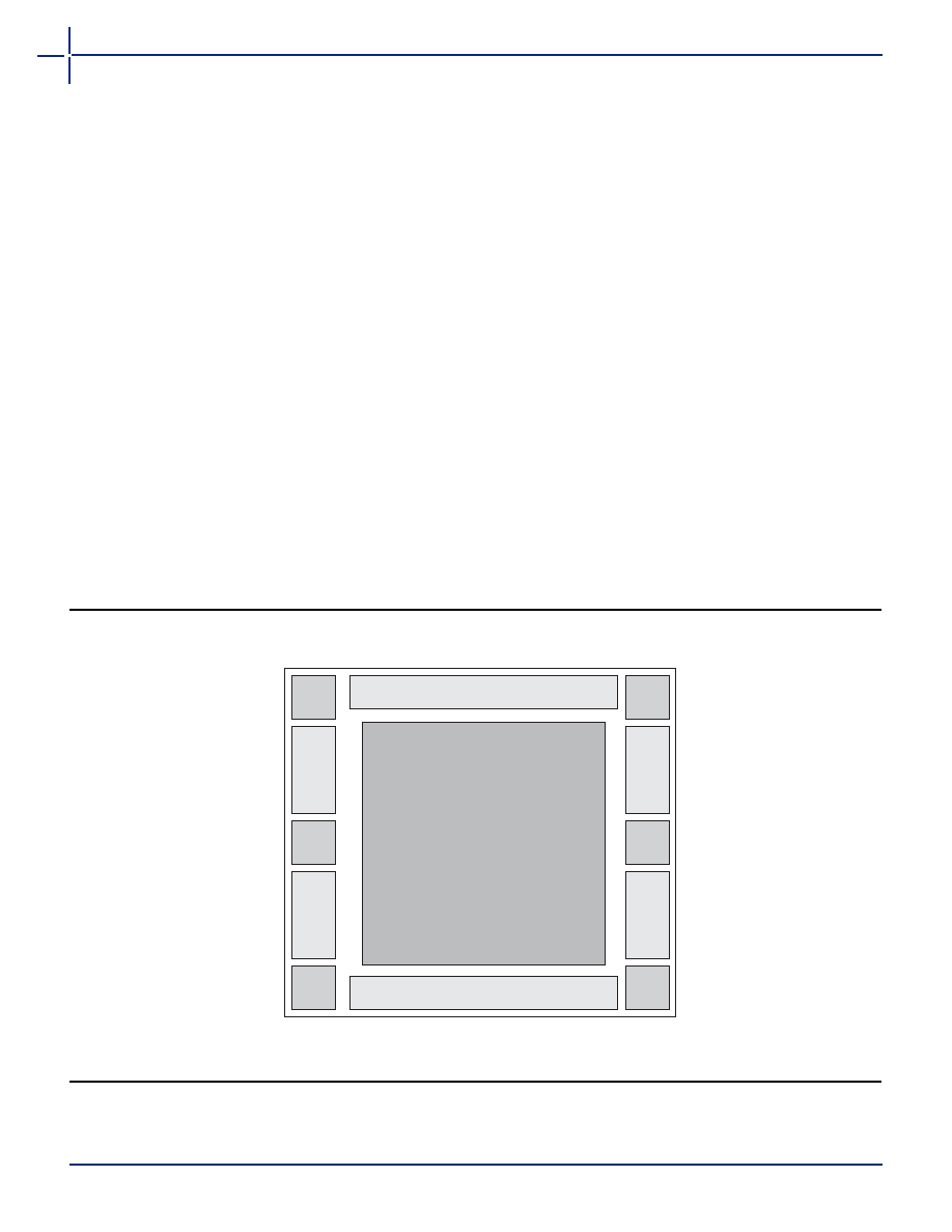
User I/O Naming Convention
Due to the comprehensive and flexible nature of IGLOO device user I/Os, a naming scheme is used to show the details
of each I/O (Figure 2-41 and Figure 2-42 on page 2-57). The name identifies to which I/O bank it belongs, as well as
pairing and pin polarity for differential I/Os.
I/O Nomenclature = FF/Gmn/IOuxwBy
Gmn is only used for I/Os that also have CCC access—i.e., global pins.
FF
= Indicates the I/O dedicated for the Flash*Freeze mode activation pin
G= Global
m
= Global pin location associated with each CCC on the device: A (northwest corner), B (northeast corner), C (east
middle), D (southeast corner), E (southwest corner), and F (west middle)
n
= Global input MUX and pin number of the associated Global location m, either A0, A1, A2, B0, B1, B2, C0, C1, or
C2. Figure 2-15 on page 2-17 shows the three input pins per clock source MUX at CCC location m.
u
= I/O pair number in the bank, starting at 00 from the northwest I/O bank and proceeding in a clockwise direction
x
= P or U (Positive), N or V (Negative) for differential pairs, or R (Regular—single-ended) for the I/Os that support
single-ended and voltage-referenced I/O standards only.
w
= D (Differential Pair), P (Pair), or S (Single-Ended). D (Differential Pair) if both members of the pair are bonded
out to adjacent pins or are separated only by one GND or NC pin; P (Pair) if both members of the pair are
bonded out but do not meet the adjacency requirement; or S (Single-Ended) if the I/O pair is not bonded out.
For Differential (D) pairs, adjacency for ball grid packages means only vertical or horizontal. Diagonal
adjacency does not meet the requirements for a true differential pair.
B
= Bank
y
= Bank number (0–3). The Bank number starts at 0 from the northwest I/O bank and proceeds in a clockwise
direction.
Note: The AGL030 device does not support a PLL (VCOMPLF and VCCPLF pins).
Figure 2-41 Naming Conventions of IGLOO Devices with Two I/O Banks – Top View
CCC
"A"
CCC
"E"
CCC/PLL
"F"
CCC
"B"
CCC
"D"
CCC
"C"
AGL030
AGL060
AGL125
GND
VCC
GND
VCCIB1
VCC
GND
VCCIB0
Bank 1
Bank 0
Bank 1
Bank 0
VCOMPLF
VCCPLF
GND
V
CC
VCCIB1
GND
VCC
VCCIB0
GND
VMV1
GNDQ
GND
V
CCI
B1
V
CCI
B1
V
CC
V
CCI
B1
V
CC
GND
VMV1
GNDQ
GND
TCK
TDI
TMS
VJTAG
TRST
TDO
VPUMP
GND
GNDQ
VMV0
GND
Vcc
GND
V
CCI
B0
V
CCI
B0
Vcc
V
CCI
B0
GND
VMV0
GNDQ
相关PDF资料 |
PDF描述 |
|---|---|
| AGL10002-FFGG484I | FPGA, 1000000 GATES, 200 MHz, PBGA484 |
| AGL10002-FFGG484 | FPGA, 1000000 GATES, 200 MHz, PBGA484 |
| AGL10002-FG144I | FPGA, 1000000 GATES, 200 MHz, PBGA144 |
| AGL10002-FG144 | FPGA, 1000000 GATES, 200 MHz, PBGA144 |
| AGL10002-FG256I | FPGA, 1000000 GATES, 200 MHz, PBGA144 |
相关代理商/技术参数 |
参数描述 |
|---|---|
| AGL1000V2-CS144 | 制造商:ACTEL 制造商全称:Actel Corporation 功能描述:IGLOO Low-Power Flash FPGAs with Flash Freeze Technology |
| AGL1000V2-CS144ES | 制造商:ACTEL 制造商全称:Actel Corporation 功能描述:IGLOO Low-Power Flash FPGAs with Flash Freeze Technology |
| AGL1000V2-CS144I | 制造商:ACTEL 制造商全称:Actel Corporation 功能描述:IGLOO Low-Power Flash FPGAs with Flash Freeze Technology |
| AGL1000V2-CS144PP | 制造商:ACTEL 制造商全称:Actel Corporation 功能描述:IGLOO Low-Power Flash FPGAs with Flash Freeze Technology |
| AGL1000V2-CS281 | 功能描述:IC FPGA 1KB FLASH 1M 281-CSP RoHS:否 类别:集成电路 (IC) >> 嵌入式 - FPGA(现场可编程门阵列) 系列:IGLOO 标准包装:40 系列:SX-A LAB/CLB数:6036 逻辑元件/单元数:- RAM 位总计:- 输入/输出数:360 门数:108000 电源电压:2.25 V ~ 5.25 V 安装类型:表面贴装 工作温度:0°C ~ 70°C 封装/外壳:484-BGA 供应商设备封装:484-FPBGA(27X27) |
发布紧急采购,3分钟左右您将得到回复。