- 您现在的位置:买卖IC网 > PDF目录362733 > Enhanced Am486 dx4 (Advanced Micro Devices, Inc.) High-Performance Design On-Chip Integration Complete 32-Bit Architecture Micrprocessor(高性能设计片上集成完全32位体系微处理器) PDF资料下载
参数资料
| 型号: | Enhanced Am486 dx4 |
| 厂商: | Advanced Micro Devices, Inc. |
| 英文描述: | High-Performance Design On-Chip Integration Complete 32-Bit Architecture Micrprocessor(高性能设计片上集成完全32位体系微处理器) |
| 中文描述: | 高性能设计的片上集成完整的32位架构Micrprocessor(高性能设计片上集成完全32位体系微处理器) |
| 文件页数: | 28/69页 |
| 文件大小: | 1068K |
| 代理商: | ENHANCED AM486 DX4 |
第1页第2页第3页第4页第5页第6页第7页第8页第9页第10页第11页第12页第13页第14页第15页第16页第17页第18页第19页第20页第21页第22页第23页第24页第25页第26页第27页当前第28页第29页第30页第31页第32页第33页第34页第35页第36页第37页第38页第39页第40页第41页第42页第43页第44页第45页第46页第47页第48页第49页第50页第51页第52页第53页第54页第55页第56页第57页第58页第59页第60页第61页第62页第63页第64页第65页第66页第67页第68页第69页
Enhanced Am486 Microprocessor
AMD
28
PRELIMINARY
Step 1 During a snoop to the on-chip cache that hits a
modified cache line, the HOLD signal cannot
be deasserted to the microprocessor until the
next clock cycle after HITM transitions active.
Step 2 After the write-back has commenced, the
HOLD signal should be asserted no earlier than
the next clock cycle after ADS goes active, and
no later than in the final BRDY of the last write.
Asserting HOLD later than the final BRDY may
allow the microprocessor to permit a pending
access to begin.
Step 3 If RDY is returned instead of BRDY during a
write-back, the HOLD signal can be reasserted
at any time starting one clock after ADS goes
active in the first transfer up to the final transfer
when RDY is asserted. Asserting RDY instead
of BRDY will not break the write-back cycle if
HOLD is asserted. The processor ignores
HOLD until the final write cycle of the write-
back.
4.8.5.2
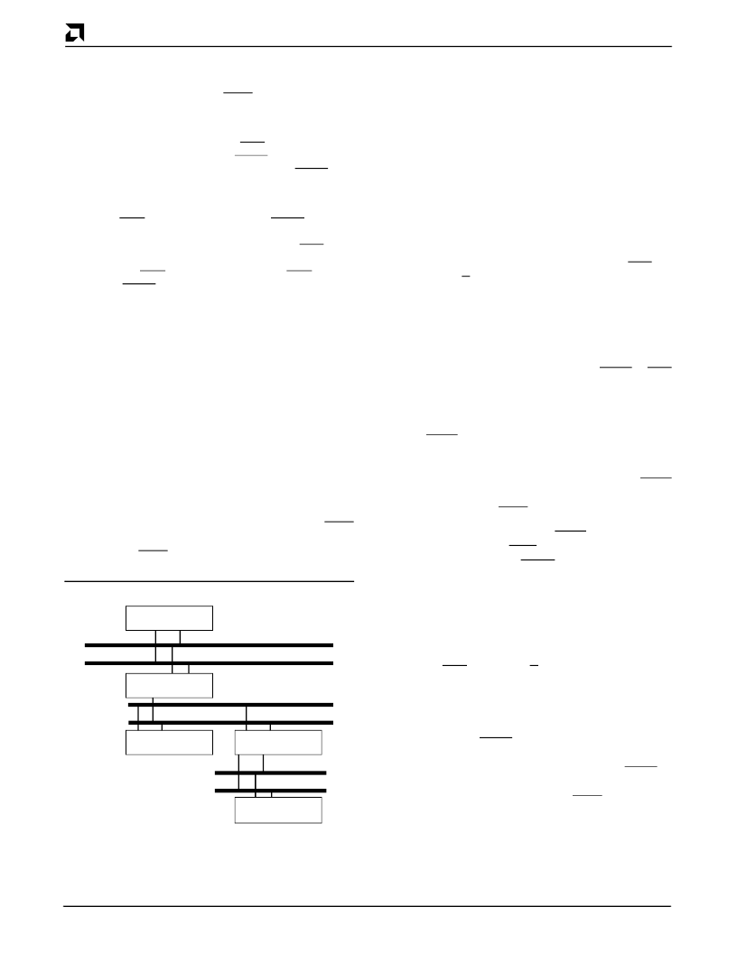
The use of AHOLD as the control mechanism is often
found in systems where an external second-level cache
is closely coupled to the microprocessor. This tight cou-
pling allows the microprocessor to operate with the least
amount of stalling from external snooping of the on-chip
cache. Additionally, snooping of the cache can be per-
formed concurrently with an access by the microproces-
sor. This feature further improves the performance of
the total system (see Figure 11).
AHOLD Bus Arbitration Implementation
Note:
To maintain proper system timing, the AHOLD
signal must remain active for one clock cycle after HITM
transitions active. Deassertion of AHOLD in the same
clock cycle as HITM assertion may ead to unpredictable
processor behavior.
DRAM
Address Bus
Data Bus
L2 Cache
Address Bus
Data Bus
I/O Bus
Interface
Slow
Peripheral
CPU
Address Bus
Data Bus
Figure 11. Closely Coupled Cache Block Diagram
The following sections describe the snooping scenarios
for the AHOLD implementation.
4.8.5.3
Scenario
: This scenario assumes that a processor-initiated
access has already started and that the external logic can
finish that access even without the address being applied after
the first clock cycle. Therefore, a snooping access with
AHOLD can be done in parallel. In this case, the processor-
initiated access is finished first, then the write-back is executed
(see Figure 12).
Normal Write-Back
The sequence is as follows:
Step 1 The processor initiates an external, simple,
non-cacheable read access, strobing ADS = 0
and W/R = 0. The address is driven from the CPU.
Step 2 In the same cycle, AHOLD is asserted to indi-
cate the start of snooping. The address bus
floats and becomes an input in the next clock
cycle.
Step 3 During the next clock cycles, the BRDY or RDY
signal is not strobed Low. Therefore, the proces-
sor-initiated access is not finished.
Step 4 Two clock cycles after AHOLD is asserted, the
EADS signal is activated to start an actual snoop-
ing cycle, and INV is valid. If INV is 0, a read access
caused the snooping cycle. If INV is 1, a write ac-
cess caused the snooping cycle. Additional EADS
are ignored due to the hit of a modified line. It is
detected after HITM goes inactive.
Step 5 Two clock cycles after EADS is asserted, the
snooping signal HITM becomes valid. The line is
modified; therefore, HITM is 0.
Step 6 In this cycle, the processor-initiated access is
finished.
Step 7 Two clock cycles after the end of the processor-
initiated access, the cache immediately starts
writing back the modified line. This is indicated
by ADS = 0 and W/R = 1. Note that AHOLD is
still active and the address bus is still an input.
However, the write-back access can be execut-
ed without any address. This is because the
corresponding address must have been on the
bus when EADS was strobed. Therefore, in the
case of the core system logic, the address for
the write-back must be latched with EADS to
be available later. This is required only if
AHOLD is not removed if HITM becomes 0.
Otherwise, the address of the write-back is put
onto the address bus by the microprocessor.
相关PDF资料 |
PDF描述 |
|---|---|
| EO12 | IRDA INFRARED TRANSCEIVER |
| EOL-62L256 | HT62L256 EOL Notification |
| EP05FA20 | FRD |
| EP05Q03L | SBD |
| EP05Q06 | SBD Type : EP05Q06 |
相关代理商/技术参数 |
参数描述 |
|---|---|
| ENHSAURR8 | 制造商:Molex 功能描述:8 PORT MACHINE MOUNT SWITCH 制造商:Molex 功能描述:COMPUTERS, NETWORK SWITCHES CONNECTIVITY, No. of Ports:8, Data Rate Max:100Mbps, |
| ENHSDURR5 | 制造商:Molex 功能描述:COMPUTERS, NETWORK SWITCHES CONNECTIVITY, No. of Ports:5, Switch Mounting:DIN Ra 制造商:Molex 功能描述:ETHERNET DIN RAIL SWITCH 5PORT |
| ENHSDURR9 | 制造商:MOLEX/WOODHEAD 功能描述:Ethernet Network Switch 制造商:Molex 功能描述:ETHERNET NETWORK SWITCH, No. of Ports:9, Data Rate Max:100Mbps, Switch Mounting: |
| ENI-110 | 功能描述:冲压机与冲模 NON-IMPACT PUNCHDOWN TOOL RoHS:否 制造商:Souriau 大小: 产品:Dies 类型:Crimping 描述/功能: |
| ENICSF2811PBKA | 制造商:Texas Instruments 功能描述: |
发布紧急采购,3分钟左右您将得到回复。