- 您现在的位置:买卖IC网 > PDF目录295886 > EP20K60EFC484-2 (ALTERA CORP) LOADABLE PLD, PBGA484 PDF资料下载
参数资料
| 型号: | EP20K60EFC484-2 |
| 厂商: | ALTERA CORP |
| 元件分类: | PLD |
| 英文描述: | LOADABLE PLD, PBGA484 |
| 封装: | 23 X 23 MM, 1 MM PITCH, FINE LINE, BGA-484 |
| 文件页数: | 44/114页 |
| 文件大小: | 4116K |
| 代理商: | EP20K60EFC484-2 |
第1页第2页第3页第4页第5页第6页第7页第8页第9页第10页第11页第12页第13页第14页第15页第16页第17页第18页第19页第20页第21页第22页第23页第24页第25页第26页第27页第28页第29页第30页第31页第32页第33页第34页第35页第36页第37页第38页第39页第40页第41页第42页第43页当前第44页第45页第46页第47页第48页第49页第50页第51页第52页第53页第54页第55页第56页第57页第58页第59页第60页第61页第62页第63页第64页第65页第66页第67页第68页第69页第70页第71页第72页第73页第74页第75页第76页第77页第78页第79页第80页第81页第82页第83页第84页第85页第86页第87页第88页第89页第90页第91页第92页第93页第94页第95页第96页第97页第98页第99页第100页第101页第102页第103页第104页第105页第106页第107页第108页第109页第110页第111页第112页第113页第114页
IGLOO nano DC and Switching Characteristics
Ad vance v0.2
2-21
Applies to IGLOO nano at 1.5 V Core Operating Conditions
Applies to IGLOO nano at 1.2 V Core Operating Conditions
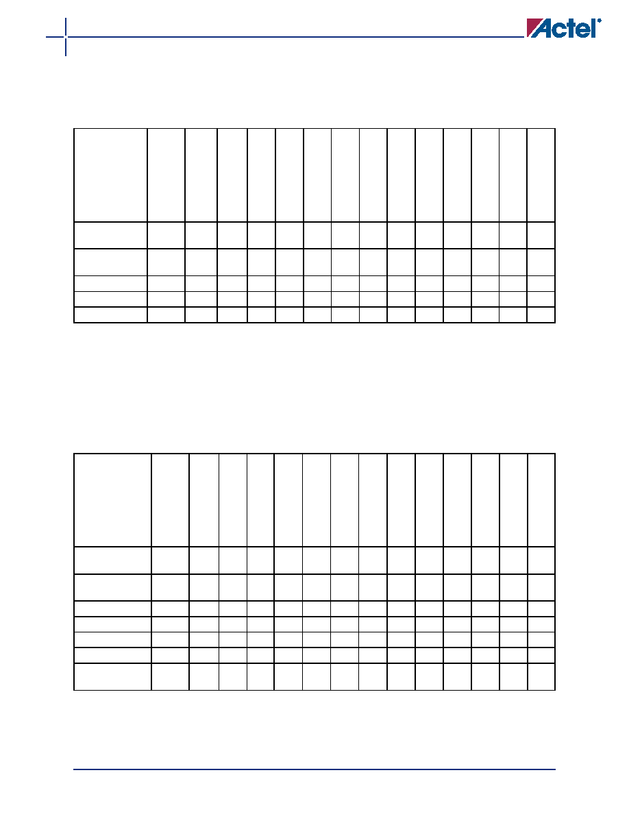
Table 2-24 Summary of I/O Timing Characteristics—Software Default Settings
STD Speed Grade, Commercial-Case Conditions: TJ = 70°C, Worst-Case VCC = 1.425 V,
Worst-Case VCCI = 3.0 V
I/O
Stand
a
rd
D
ri
v
e
St
re
n
g
th
(m
A)
Slew
Rate
Capacitive
Load
(pF)
t DO
UT
t DP
t DI
N
t PY
t PYS
t EO
UT
t ZL
t ZH
t LZ
t HZ
Unit
s
3.3 V LVTTL /
3.3 V LVCMOS
8 mA
High
5 pF
0.97
1.96
0.19
0.85
1.14
0.66
1.73
1.32
2.04
2.38
ns
3.3 V LVCMOS
Wide Range
Any 1
High
5 pF
TBD
2.5 V LVCMOS
8 mA
High
5 pF
0.97
1.99
0.19
1.06
1.22
0.66
1.76
1.42
2.04
2.25
ns
1.8 V LVCMOS
4 mA
High
5 pF
0.97
2.30
0.19
0.99
1.43
0.66
2.01
1.64
2.08
2.15
ns
1.5 V LVCMOS
2 mA
High
5 pF
0.97
2.65
0.19
1.15
1.62
0.66
2.31
1.85
2.13
2.11
ns
Notes:
1. All LVCMOS 3.3 V software macros support LVCMOS 3.3 V wide range, as specified in the JESD8-B
specification.
2. For specific junction temperature and voltage supply levels, refer to Table 2-6 on page 2-6 for derating
values.
Table 2-25 Summary of I/O Timing Characteristics—Software Default Settings
STD Speed Grade, Commercial-Case Conditions: TJ = 70°C, Worst-Case VCC = 1.14 V,
Worst-Case VCCI = 3.0 V
I/O
St
andar
d
Drive
St
re
ngth
(mA)
Slew
Ra
te
Ca
pa
ci
ti
ve
Loa
d
(pF)
t DO
U
T
t DP
t DI
N
t PY
)
t PYS
t EO
U
T
t ZL
t ZH
t LZ
t HZ
Unit
s
3.3 V LVTTL /
3.3 V LVCMOS
8 mA
High
5 pF
1.55
2.81
0.26
0.99
1.14
1.10
2.53
2.01
2.48
3.10
ns
3.3 V LVCMOS
Wide Range
Any 1
High
5 pF
TBD
ns
2.5 V LVCMOS
8 mA
High
5 pF
1.55
2.82
0.26
1.20
1.22
1.10
2.53
2.15
2.46
2.93
ns
1.8 V LVCMOS
4 mA
High
5 pF
1.55
3.11
0.26
1.12
1.43
1.10
2.76
2.46
2.49
2.75
ns
1.5 V LVCMOS
2 mA
High
5 pF
1.55
3.50
0.26
1.26
1.62
1.10
3.09
2.76
2.53
2.67
ns
1.2 V LVCMOS
1 mA
High
5 pF
1.55
4.47
0.26
1.56
1.66
1.10
3.56
3.18
3.00
3.25
ns
1.2 V LVCMOS
Wide Range
100 A High
5 pF
TBD
ns
Notes:
1. All LVCMOS 3.3 V software macros support LVCMOS 3.3 V wide range, as specified in the JESD8-B
specification.
2. For specific junction temperature and voltage supply levels, refer to Table 2-6 on page 2-6 for derating
values.
相关PDF资料 |
PDF描述 |
|---|---|
| EP20K60EFC484-3 | LOADABLE PLD, PBGA484 |
| EP20K60EFC484 | LOADABLE PLD, PBGA484 |
| EP20K60EFC672-1 | LOADABLE PLD, PBGA672 |
| EP20K60EFC672-2 | LOADABLE PLD, PBGA672 |
| EP20K60EFC672-3 | LOADABLE PLD, PBGA672 |
相关代理商/技术参数 |
参数描述 |
|---|---|
| EP20K60EFI144-1ES | 制造商:未知厂家 制造商全称:未知厂家 功能描述:FPGA |
| EP20K60EFI144-2ES | 制造商:未知厂家 制造商全称:未知厂家 功能描述:FPGA |
| EP20K60EFI144-3ES | 制造商:未知厂家 制造商全称:未知厂家 功能描述:FPGA |
| EP20K60EFI324-1ES | 制造商:未知厂家 制造商全称:未知厂家 功能描述:FPGA |
| EP20K60EFI324-2ES | 制造商:未知厂家 制造商全称:未知厂家 功能描述:FPGA |
发布紧急采购,3分钟左右您将得到回复。