- 您现在的位置:买卖IC网 > PDF目录295886 > EP20K60EFC484-2 (ALTERA CORP) LOADABLE PLD, PBGA484 PDF资料下载
参数资料
| 型号: | EP20K60EFC484-2 |
| 厂商: | ALTERA CORP |
| 元件分类: | PLD |
| 英文描述: | LOADABLE PLD, PBGA484 |
| 封装: | 23 X 23 MM, 1 MM PITCH, FINE LINE, BGA-484 |
| 文件页数: | 53/114页 |
| 文件大小: | 4116K |
| 代理商: | EP20K60EFC484-2 |
第1页第2页第3页第4页第5页第6页第7页第8页第9页第10页第11页第12页第13页第14页第15页第16页第17页第18页第19页第20页第21页第22页第23页第24页第25页第26页第27页第28页第29页第30页第31页第32页第33页第34页第35页第36页第37页第38页第39页第40页第41页第42页第43页第44页第45页第46页第47页第48页第49页第50页第51页第52页当前第53页第54页第55页第56页第57页第58页第59页第60页第61页第62页第63页第64页第65页第66页第67页第68页第69页第70页第71页第72页第73页第74页第75页第76页第77页第78页第79页第80页第81页第82页第83页第84页第85页第86页第87页第88页第89页第90页第91页第92页第93页第94页第95页第96页第97页第98页第99页第100页第101页第102页第103页第104页第105页第106页第107页第108页第109页第110页第111页第112页第113页第114页
IGLOO nano DC and Switching Characteristics
Ad vance v0.2
2-29
2.5 V LVCMOS
Low-Voltage CMOS for 2.5 V is an extension of the LVCMOS standard (JESD8-5) used for general-
purpose 2.5 V applications. It uses a 5 V–tolerant input buffer and push-pull output buffer.
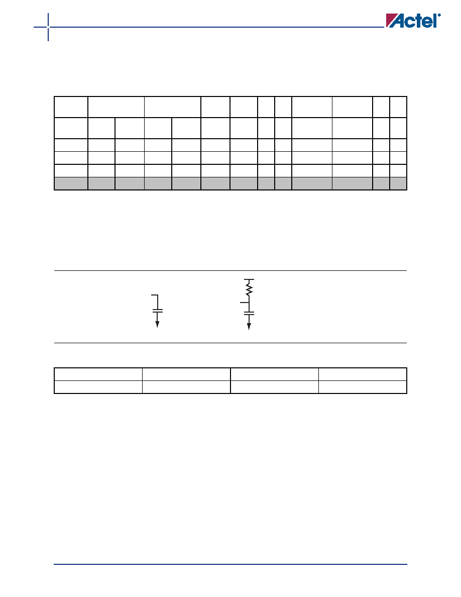
Table 2-40 Minimum and Maximum DC Input and Output Levels
2.5 V
LVCMOS
VIL
VIH
VOL
VOH
IOL IOH
IOSL
IOSH
IIL
1
IIH
2
Drive
Strength
Min., V Max., V Min., V Max., V Max., V Min., V mA mA Max., mA3
Max., mA3 A4 A4
2 mA
–0.3
0.7
1.7
3.6
0.7
1.7
2
16
18
10
4 mA
–0.3
0.7
1.7
3.6
0.7
1.7
4
16
18
10
6 mA
–0.3
0.7
1.7
3.6
0.7
1.7
6
32
37
10
8 mA
–0.3
0.7
1.7
3.6
0.7
1.7
8
32
37
10
Notes:
1. IIL is the input leakage current per I/O pin over recommended operating conditions where –0.3 < VIN < VIL.
2. IIH is the input leakage current per I/O pin over recommended operating conditions where VIH < VIN < VCCI.
Input current is larger when operating outside recommended ranges.
3. Currents are measured at high temperature (100°C junction temperature) and maximum voltage.
4. Currents are measured at 85°C junction temperature.
5. Software default selection highlighted in gray.
Figure 2-8 AC Loading
Table 2-41 2.5 V LVCMOS AC Waveforms, Measuring Points, and Capacitive Loads
Input LOW (V)
Input HIGH (V)
Measuring Point* (V)
CLOAD (pF)
02.5
1.2
5
Test Point
Enable Path
Datapath
5 pF
R = 1 k
R to VCCI for tLZ/tZL/tZLS
R to GND for tHZ/tZH/tZHS
35 pF for tZH/tZHS/tZL/tZLS
5 pF for tHZ/tLZ
相关PDF资料 |
PDF描述 |
|---|---|
| EP20K60EFC484-3 | LOADABLE PLD, PBGA484 |
| EP20K60EFC484 | LOADABLE PLD, PBGA484 |
| EP20K60EFC672-1 | LOADABLE PLD, PBGA672 |
| EP20K60EFC672-2 | LOADABLE PLD, PBGA672 |
| EP20K60EFC672-3 | LOADABLE PLD, PBGA672 |
相关代理商/技术参数 |
参数描述 |
|---|---|
| EP20K60EFI144-1ES | 制造商:未知厂家 制造商全称:未知厂家 功能描述:FPGA |
| EP20K60EFI144-2ES | 制造商:未知厂家 制造商全称:未知厂家 功能描述:FPGA |
| EP20K60EFI144-3ES | 制造商:未知厂家 制造商全称:未知厂家 功能描述:FPGA |
| EP20K60EFI324-1ES | 制造商:未知厂家 制造商全称:未知厂家 功能描述:FPGA |
| EP20K60EFI324-2ES | 制造商:未知厂家 制造商全称:未知厂家 功能描述:FPGA |
发布紧急采购,3分钟左右您将得到回复。