- 您现在的位置:买卖IC网 > PDF目录295886 > EP20K60EFC484-2 (ALTERA CORP) LOADABLE PLD, PBGA484 PDF资料下载
参数资料
| 型号: | EP20K60EFC484-2 |
| 厂商: | ALTERA CORP |
| 元件分类: | PLD |
| 英文描述: | LOADABLE PLD, PBGA484 |
| 封装: | 23 X 23 MM, 1 MM PITCH, FINE LINE, BGA-484 |
| 文件页数: | 90/114页 |
| 文件大小: | 4116K |
| 代理商: | EP20K60EFC484-2 |
第1页第2页第3页第4页第5页第6页第7页第8页第9页第10页第11页第12页第13页第14页第15页第16页第17页第18页第19页第20页第21页第22页第23页第24页第25页第26页第27页第28页第29页第30页第31页第32页第33页第34页第35页第36页第37页第38页第39页第40页第41页第42页第43页第44页第45页第46页第47页第48页第49页第50页第51页第52页第53页第54页第55页第56页第57页第58页第59页第60页第61页第62页第63页第64页第65页第66页第67页第68页第69页第70页第71页第72页第73页第74页第75页第76页第77页第78页第79页第80页第81页第82页第83页第84页第85页第86页第87页第88页第89页当前第90页第91页第92页第93页第94页第95页第96页第97页第98页第99页第100页第101页第102页第103页第104页第105页第106页第107页第108页第109页第110页第111页第112页第113页第114页
IGLOO nano DC and Switching Characteristics
Ad vance v0.2
2-63
1.2 V DC Core Voltage
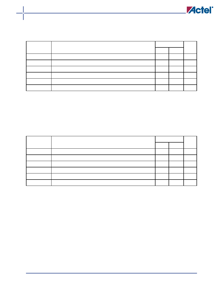
Table 2-86 AGLN010 Global Resource
Commercial-Case Conditions: TJ = 70°C, VCC = 1.14 V
Parameter
Description
Std.
Units
Min.1
Max.2
tRCKL
Input LOW Delay for Global Clock
TBD
ns
tRCKH
Input HIGH Delay for Global Clock
TBD
ns
tRCKMPWH
Minimum Pulse Width HIGH for Global Clock
ns
tRCKMPWL
Minimum Pulse Width LOW for Global Clock
ns
tRCKSW
Maximum Skew for Global Clock
TBD
ns
FRMAX
Maximum Frequency for Global Clock
MHz
Notes:
1. Value reflects minimum load. The delay is measured from the CCC output to the clock pin of a sequential
element, located in a lightly loaded row (single element is connected to the global net).
2. Value reflects maximum load. The delay is measured on the clock pin of the farthest sequential element,
located in a fully loaded row (all available flip-flops are connected to the global net in the row).
3. For specific junction temperature and voltage supply levels, refer to Table 2-7 on page 2-7 for derating
values.
Table 2-87 AGLN015 Global Resource
Commercial-Case Conditions: TJ = 70°C, VCC = 1.14 V
Parameter
Description
Std.
Units
Min.1
Max.2
tRCKL
Input LOW Delay for Global Clock
TBD
ns
tRCKH
Input HIGH Delay for Global Clock
TBD
ns
tRCKMPWH
Minimum Pulse Width HIGH for Global Clock
ns
tRCKMPWL
Minimum Pulse Width LOW for Global Clock
ns
tRCKSW
Maximum Skew for Global Clock
TBD
ns
FRMAX
Maximum Frequency for Global Clock
MHz
Notes:
1. Value reflects minimum load. The delay is measured from the CCC output to the clock pin of a sequential
element, located in a lightly loaded row (single element is connected to the global net).
2. Value reflects maximum load. The delay is measured on the clock pin of the farthest sequential element,
located in a fully loaded row (all available flip-flops are connected to the global net in the row).
3. For specific junction temperature and voltage supply levels, refer to Table 2-7 on page 2-7 for derating
values.
相关PDF资料 |
PDF描述 |
|---|---|
| EP20K60EFC484-3 | LOADABLE PLD, PBGA484 |
| EP20K60EFC484 | LOADABLE PLD, PBGA484 |
| EP20K60EFC672-1 | LOADABLE PLD, PBGA672 |
| EP20K60EFC672-2 | LOADABLE PLD, PBGA672 |
| EP20K60EFC672-3 | LOADABLE PLD, PBGA672 |
相关代理商/技术参数 |
参数描述 |
|---|---|
| EP20K60EFI144-1ES | 制造商:未知厂家 制造商全称:未知厂家 功能描述:FPGA |
| EP20K60EFI144-2ES | 制造商:未知厂家 制造商全称:未知厂家 功能描述:FPGA |
| EP20K60EFI144-3ES | 制造商:未知厂家 制造商全称:未知厂家 功能描述:FPGA |
| EP20K60EFI324-1ES | 制造商:未知厂家 制造商全称:未知厂家 功能描述:FPGA |
| EP20K60EFI324-2ES | 制造商:未知厂家 制造商全称:未知厂家 功能描述:FPGA |
发布紧急采购,3分钟左右您将得到回复。