- 您现在的位置:买卖IC网 > PDF目录295886 > EP20K60EFC484-2 (ALTERA CORP) LOADABLE PLD, PBGA484 PDF资料下载
参数资料
| 型号: | EP20K60EFC484-2 |
| 厂商: | ALTERA CORP |
| 元件分类: | PLD |
| 英文描述: | LOADABLE PLD, PBGA484 |
| 封装: | 23 X 23 MM, 1 MM PITCH, FINE LINE, BGA-484 |
| 文件页数: | 81/114页 |
| 文件大小: | 4116K |
| 代理商: | EP20K60EFC484-2 |
第1页第2页第3页第4页第5页第6页第7页第8页第9页第10页第11页第12页第13页第14页第15页第16页第17页第18页第19页第20页第21页第22页第23页第24页第25页第26页第27页第28页第29页第30页第31页第32页第33页第34页第35页第36页第37页第38页第39页第40页第41页第42页第43页第44页第45页第46页第47页第48页第49页第50页第51页第52页第53页第54页第55页第56页第57页第58页第59页第60页第61页第62页第63页第64页第65页第66页第67页第68页第69页第70页第71页第72页第73页第74页第75页第76页第77页第78页第79页第80页当前第81页第82页第83页第84页第85页第86页第87页第88页第89页第90页第91页第92页第93页第94页第95页第96页第97页第98页第99页第100页第101页第102页第103页第104页第105页第106页第107页第108页第109页第110页第111页第112页第113页第114页
IGLOO nano DC and Switching Characteristics
Ad vance v0.2
2-55
Timing Characteristics
1.5 V DC Core Voltage
1.2 V DC Core Voltage
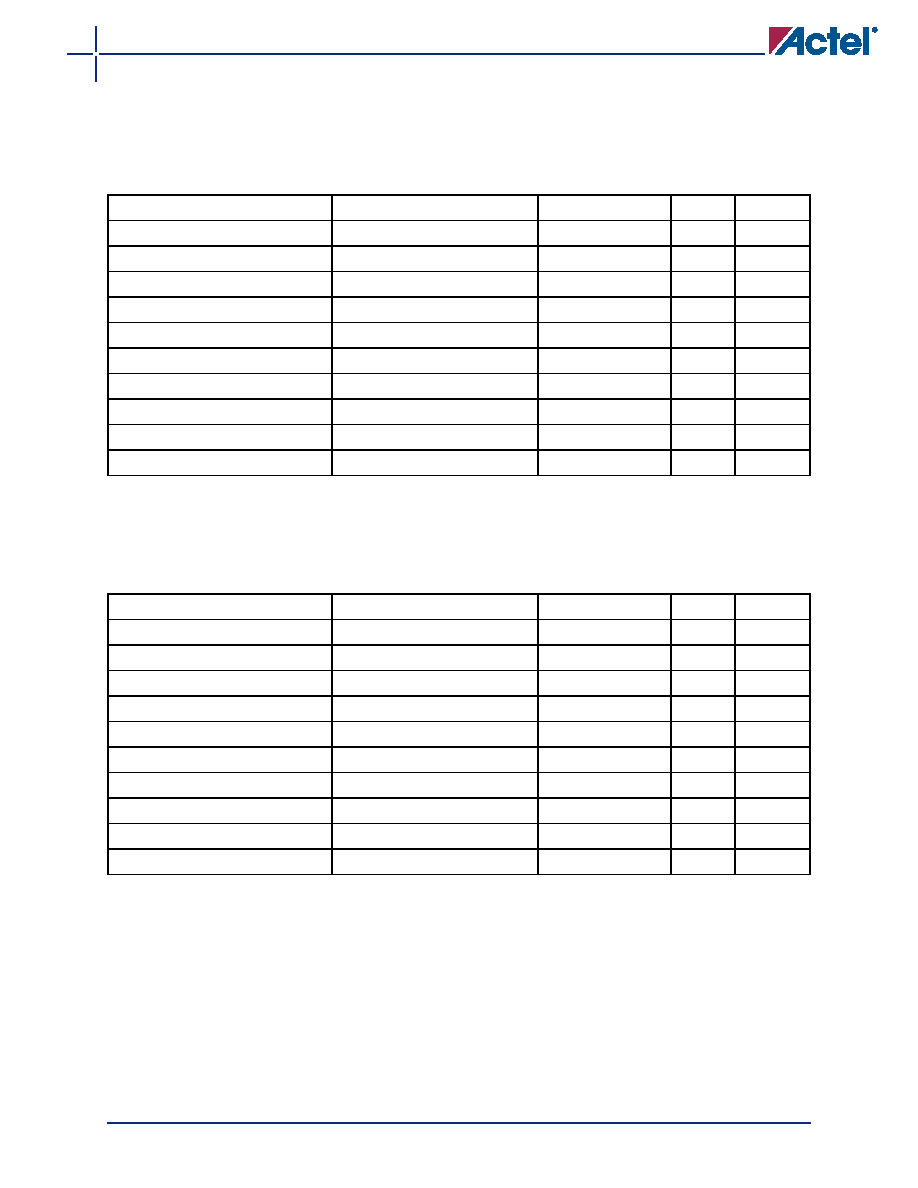
Table 2-76 Combinatorial Cell Propagation Delays
Commercial-Case Conditions: TJ = 70°C, Worst-Case VCC = 1.425 V
Combinatorial Cell
Equation
Parameter
Std.
Units
INV
Y = !A
tPD
0.76
ns
AND2
Y = A B
tPD
0.87
ns
NAND2
Y = !(A B)
tPD
0.91
ns
OR2
Y = A + B
tPD
0.90
ns
NOR2
Y = !(A + B)
tPD
0.94
ns
XOR2
Y = A
⊕ Bt
PD
1.39
ns
MAJ3
Y = MAJ(A, B, C)
tPD
1.44
ns
XOR3
Y = A
⊕ B ⊕ Ct
PD
1.60
ns
MUX2
Y = A !S + B S
tPD
1.17
ns
AND3
Y = A B C
tPD
1.18
ns
Note: For specific junction temperature and voltage supply levels, refer to Table 2-6 on page 2-6 for derating
values.
Table 2-77 Combinatorial Cell Propagation Delays
Commercial-Case Conditions: TJ = 70°C, Worst-Case VCC = 1.14 V
Combinatorial Cell
Equation
Parameter
Std.
Units
INV
Y = !A
tPD
1.33
ns
AND2
Y = A B
tPD
1.48
ns
NAND2
Y = !(A B)
tPD
1.58
ns
OR2
Y = A + B
tPD
1.53
ns
NOR2
Y = !(A + B)
tPD
1.63
ns
XOR2
Y = A
⊕ Bt
PD
2.34
ns
MAJ3
Y = MAJ(A, B, C)
tPD
2.59
ns
XOR3
Y = A
⊕ B ⊕ Ct
PD
2.74
ns
MUX2
Y = A !S + B S
tPD
2.03
ns
AND3
Y = A B C
tPD
2.11
ns
Note: For specific junction temperature and voltage supply levels, refer to Table 2-7 on page 2-7 for derating
values.
相关PDF资料 |
PDF描述 |
|---|---|
| EP20K60EFC484-3 | LOADABLE PLD, PBGA484 |
| EP20K60EFC484 | LOADABLE PLD, PBGA484 |
| EP20K60EFC672-1 | LOADABLE PLD, PBGA672 |
| EP20K60EFC672-2 | LOADABLE PLD, PBGA672 |
| EP20K60EFC672-3 | LOADABLE PLD, PBGA672 |
相关代理商/技术参数 |
参数描述 |
|---|---|
| EP20K60EFI144-1ES | 制造商:未知厂家 制造商全称:未知厂家 功能描述:FPGA |
| EP20K60EFI144-2ES | 制造商:未知厂家 制造商全称:未知厂家 功能描述:FPGA |
| EP20K60EFI144-3ES | 制造商:未知厂家 制造商全称:未知厂家 功能描述:FPGA |
| EP20K60EFI324-1ES | 制造商:未知厂家 制造商全称:未知厂家 功能描述:FPGA |
| EP20K60EFI324-2ES | 制造商:未知厂家 制造商全称:未知厂家 功能描述:FPGA |
发布紧急采购,3分钟左右您将得到回复。