- 您现在的位置:买卖IC网 > PDF目录295887 > EP2C20F256I6N (ALTERA CORP) FPGA, 1196 CLBS, PBGA256 PDF资料下载
参数资料
| 型号: | EP2C20F256I6N |
| 厂商: | ALTERA CORP |
| 元件分类: | FPGA |
| 英文描述: | FPGA, 1196 CLBS, PBGA256 |
| 封装: | LEAD FREE, FBGA-256 |
| 文件页数: | 168/168页 |
| 文件大小: | 2206K |
| 代理商: | EP2C20F256I6N |
第1页第2页第3页第4页第5页第6页第7页第8页第9页第10页第11页第12页第13页第14页第15页第16页第17页第18页第19页第20页第21页第22页第23页第24页第25页第26页第27页第28页第29页第30页第31页第32页第33页第34页第35页第36页第37页第38页第39页第40页第41页第42页第43页第44页第45页第46页第47页第48页第49页第50页第51页第52页第53页第54页第55页第56页第57页第58页第59页第60页第61页第62页第63页第64页第65页第66页第67页第68页第69页第70页第71页第72页第73页第74页第75页第76页第77页第78页第79页第80页第81页第82页第83页第84页第85页第86页第87页第88页第89页第90页第91页第92页第93页第94页第95页第96页第97页第98页第99页第100页第101页第102页第103页第104页第105页第106页第107页第108页第109页第110页第111页第112页第113页第114页第115页第116页第117页第118页第119页第120页第121页第122页第123页第124页第125页第126页第127页第128页第129页第130页第131页第132页第133页第134页第135页第136页第137页第138页第139页第140页第141页第142页第143页第144页第145页第146页第147页第148页第149页第150页第151页第152页第153页第154页第155页第156页第157页第158页第159页第160页第161页第162页第163页第164页第165页第166页第167页当前第168页
Altera Corporation
5–9
February 2008
Cyclone II Device Handbook, Volume 1
DC Characteristics and Timing Specifications
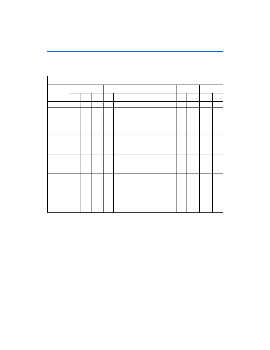
Table 5–8 shows the recommended operating conditions for user I/O
pins with differential I/O standards.
Table 5–8. Recommended Operating Conditions for User I/O Pins Using Differential Signal I/O Standards
I/O
Standard
VCCIO (V)
VICM (V)
VIL (V)
VIH (V)
Min
Typ
Max
Min
Typ
Max
Min
Typ
Max
Min
Max
Min
Max
LVDS
2.375
2.5
2.625
0.1
—
0.65
0.1
—
2.0
—
Mini-LVDS
2.375
2.5
2.625
—
————
—
RSDS (2)
2.375
2.5
2.625
—
————
—
LVPECL
3.135
3.3
3.465
0.1
0.6
0.95
—
0
2.2
2.1
2.88
Differential
1.5-V HSTL
class I
and II (4)
1.425
1.5
1.575
0.2
—
VCCIO
+ 0.6
0.68
—
0.9
—
VREF
– 0.20
VREF
+ 0.20
—
Differential
1.8-V HSTL
class I
and II (4)
1.71
1.8
1.89
—
————
—
VREF
– 0.20
VREF
+ 0.20
—
Differential
SSTL-2
class I
and II (5)
2.375
2.5
2.625
0.36
—
VCCIO
+ 0.6
0.5 ×
VCCIO
– 0.2
0.5 ×
VCCIO
0.5 ×
VCCIO
+ 0.2
—VREF
– 0.35
VREF
+ 0.35
—
Differential
SSTL-18
class I
and II (5)
1.7
1.8
1.9
0.25
—
VCCIO
+ 0.6
0.5 ×
VCCIO
– 0.2
0.5 ×
VCCIO
0.5 ×
VCCIO
+ 0.2
—VREF
– 0.25
VREF
+ 0.25
—
Notes to Table 5–8:
(1)
Refer to the High-Speed Differential Interfaces in Cyclone II Devices chapter of the Cyclone II Device Handbook for
measurement conditions on VID.
(2)
The RSDS and mini-LVDS I/O standards are only supported on output pins.
(3)
The LVPECL I/O standard is only supported on clock input pins. This I/O standard is not supported on output
pins.
(4)
The differential 1.8-V and 1.5-V HSTL I/O standards are only supported on clock input pins and PLL output clock
pins.
(5)
The differential SSTL-18 and SSTL-2 I/O standards are only supported on clock input pins and PLL output clock
pins.
(6)
The LVPECL clock inputs are powered by VCCINT and support all VCCIO settings. However, it is recommended to
connect VCCIO to typical value of 3.3V.
相关PDF资料 |
PDF描述 |
|---|---|
| EP2SGX60CF780C3N | FPGA, 60440 CLBS, 717 MHz, PBGA780 |
| EP2SGX60CF780C3 | FPGA, 60440 CLBS, 717 MHz, PBGA780 |
| EP2SGX60CF780C4N | FPGA, 60440 CLBS, 717 MHz, PBGA780 |
| EP2SGX60CF780C4 | FPGA, 60440 CLBS, 717 MHz, PBGA780 |
| EP2SGX60CF780C5N | FPGA, 60440 CLBS, 640 MHz, PBGA780 |
相关代理商/技术参数 |
参数描述 |
|---|---|
| EP2C20F256I8 | 功能描述:FPGA - 现场可编程门阵列 FPGA - Cyclone II 1172 LABs 152 IOs RoHS:否 制造商:Altera Corporation 系列:Cyclone V E 栅极数量: 逻辑块数量:943 内嵌式块RAM - EBR:1956 kbit 输入/输出端数量:128 最大工作频率:800 MHz 工作电源电压:1.1 V 最大工作温度:+ 70 C 安装风格:SMD/SMT 封装 / 箱体:FBGA-256 |
| EP2C20F256I8GA | 制造商:Altera Corporation 功能描述: |
| EP2C20F256I8N | 功能描述:FPGA - 现场可编程门阵列 FPGA - Cyclone II 1172 LABs 152 IOs RoHS:否 制造商:Altera Corporation 系列:Cyclone V E 栅极数量: 逻辑块数量:943 内嵌式块RAM - EBR:1956 kbit 输入/输出端数量:128 最大工作频率:800 MHz 工作电源电压:1.1 V 最大工作温度:+ 70 C 安装风格:SMD/SMT 封装 / 箱体:FBGA-256 |
| EP2C20F484C6 | 功能描述:FPGA - 现场可编程门阵列 FPGA - Cyclone II 1172 LABs 315 IOs RoHS:否 制造商:Altera Corporation 系列:Cyclone V E 栅极数量: 逻辑块数量:943 内嵌式块RAM - EBR:1956 kbit 输入/输出端数量:128 最大工作频率:800 MHz 工作电源电压:1.1 V 最大工作温度:+ 70 C 安装风格:SMD/SMT 封装 / 箱体:FBGA-256 |
| EP2C20F484C6N | 功能描述:FPGA - 现场可编程门阵列 FPGA - Cyclone II 1172 LABs 315 IOs RoHS:否 制造商:Altera Corporation 系列:Cyclone V E 栅极数量: 逻辑块数量:943 内嵌式块RAM - EBR:1956 kbit 输入/输出端数量:128 最大工作频率:800 MHz 工作电源电压:1.1 V 最大工作温度:+ 70 C 安装风格:SMD/SMT 封装 / 箱体:FBGA-256 |
发布紧急采购,3分钟左右您将得到回复。