- 您现在的位置:买卖IC网 > PDF目录261241 > IBM25EMPPC750EBUF2000 32-BIT, 200 MHz, RISC PROCESSOR, CBGA360 PDF资料下载
参数资料
| 型号: | IBM25EMPPC750EBUF2000 |
| 元件分类: | 微控制器/微处理器 |
| 英文描述: | 32-BIT, 200 MHz, RISC PROCESSOR, CBGA360 |
| 封装: | 25 X 25 MM, 1.27 MM PITCH, CERAMIC, BGA-360 |
| 文件页数: | 26/43页 |
| 文件大小: | 431K |
| 代理商: | IBM25EMPPC750EBUF2000 |
第1页第2页第3页第4页第5页第6页第7页第8页第9页第10页第11页第12页第13页第14页第15页第16页第17页第18页第19页第20页第21页第22页第23页第24页第25页当前第26页第27页第28页第29页第30页第31页第32页第33页第34页第35页第36页第37页第38页第39页第40页第41页第42页第43页
Preliminary and subject to change without notice
PPC740 and PPC750 Hardware Specifications
32 of 43
“Clock AC Specications“ for valid SYSCLK and VCO frequencies.
3. In PLL-bypass mode, the SYSCLK input signal clocks the internal processor directly, the PLL is dis-
abled, and the bus mode is set for 1:1 mode operation. This mode is intended for factory use only.
Note: The AC timing specications given in the document do not apply in PLL-bypass mode.
4. In Clock - off mode, no clocking occurs inside the PPC740 or PPC750 regardless of the SYSCLK input.
5. This limit is 83.3 MHz as specied in Section 3.1.2.1, “Clock AC Specications“.
Table 17 provides sample core-to-L2 frequencies.
Note:
1. Although the PPC750 is designed for L2 bus ratios of 1:1, 1.5:1, 2:1, 2.5:1 and 3:1, this specication
supports the L2 frequency range specied in Section 3.1.2.4, “L2 Clock AC Specications“. For higher
L2 frequencies not supported in this document, please contact your IBM marketing representative.
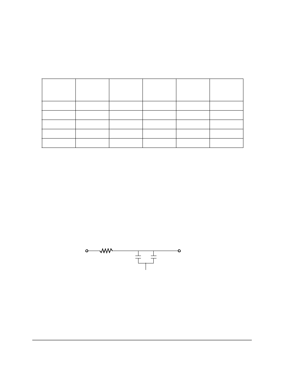
7.2 PLL Power Supply Filtering
The AVdd and L2AVdd power signals are provided on the PPC740 and PPC750 to pro-
vide power to the clock generation phase-locked loop and L2 cache delay-locked loop
respectively. To ensure stability of the internal clock, the power supplied to the AVdd
input signal should be ltered using a circuit similar to the one shown in Figure 17 .
The circuit should be placed as close as possible to the AVdd pin to ensure it lters out
as much noise as possible. An identical but separate circuit should be placed as close
as possible to the L2AVdd pin.
Figure 17. PLL Power Supply Filter Circuit
7.3 Decoupling Recommendations
Due to the PPC740’s and PPC750’s dynamic power management feature, large address
and data buses, and high operating frequencies, the PPC740 and PPC750 can generate
transient power surges and high frequency noise in its power supply, especially while
driving large capacitive loads. This noise must be prevented from reaching other com-
Table 17. Sample Core-to-L2 Frequencies1
Core
Frequency
in MHz
÷1
÷1.5
÷2
÷2.5
÷3
200
—
133.3
100
80
—
225
—
112.5
90
—
233
—
116.5
93.2
—
250
—
125
100
83.3
266
—
133
106.4
88.6
VDD
AVDD (or L2AVdd)
10
10
F
0.1
F
GND
相关PDF资料 |
PDF描述 |
|---|---|
| ICS2494AM-XXX | 135 MHz, VIDEO CLOCK GENERATOR, PDSO20 |
| ICS650R-14IT | 133.33 MHz, OTHER CLOCK GENERATOR, PDSO20 |
| ICS650R-14T | 133.33 MHz, OTHER CLOCK GENERATOR, PDSO20 |
| ICS840001AKI-34LF | 213.33 MHz, OTHER CLOCK GENERATOR, QCC16 |
| I2041AG-8TR | 40.4 MHz, OTHER CLOCK GENERATOR, PDSO8 |
相关代理商/技术参数 |
参数描述 |
|---|---|
| IBM25EMPPC750LEBA300 | 制造商:未知厂家 制造商全称:未知厂家 功能描述:32-Bit Microprocessor |
| IBM25EMPPC750LEBA333 | 制造商:未知厂家 制造商全称:未知厂家 功能描述:32-Bit Microprocessor |
| IBM25EMPPC750LEBA366 | 制造商:未知厂家 制造商全称:未知厂家 功能描述:32-Bit Microprocessor |
| IBM25EMPPC750LEBA400 | 制造商:未知厂家 制造商全称:未知厂家 功能描述:32-Bit Microprocessor |
| IBM25EMPPC750LEBA466 | 制造商:未知厂家 制造商全称:未知厂家 功能描述:32-Bit Microprocessor |
发布紧急采购,3分钟左右您将得到回复。