- 您现在的位置:买卖IC网 > PDF目录261241 > IBM25EMPPC750EBUF2000 32-BIT, 200 MHz, RISC PROCESSOR, CBGA360 PDF资料下载
参数资料
| 型号: | IBM25EMPPC750EBUF2000 |
| 元件分类: | 微控制器/微处理器 |
| 英文描述: | 32-BIT, 200 MHz, RISC PROCESSOR, CBGA360 |
| 封装: | 25 X 25 MM, 1.27 MM PITCH, CERAMIC, BGA-360 |
| 文件页数: | 4/43页 |
| 文件大小: | 431K |
| 代理商: | IBM25EMPPC750EBUF2000 |
第1页第2页第3页当前第4页第5页第6页第7页第8页第9页第10页第11页第12页第13页第14页第15页第16页第17页第18页第19页第20页第21页第22页第23页第24页第25页第26页第27页第28页第29页第30页第31页第32页第33页第34页第35页第36页第37页第38页第39页第40页第41页第42页第43页
Preliminary and subject to change without notice
PPC740 and PPC750 Hardware Specifications
12 of 43
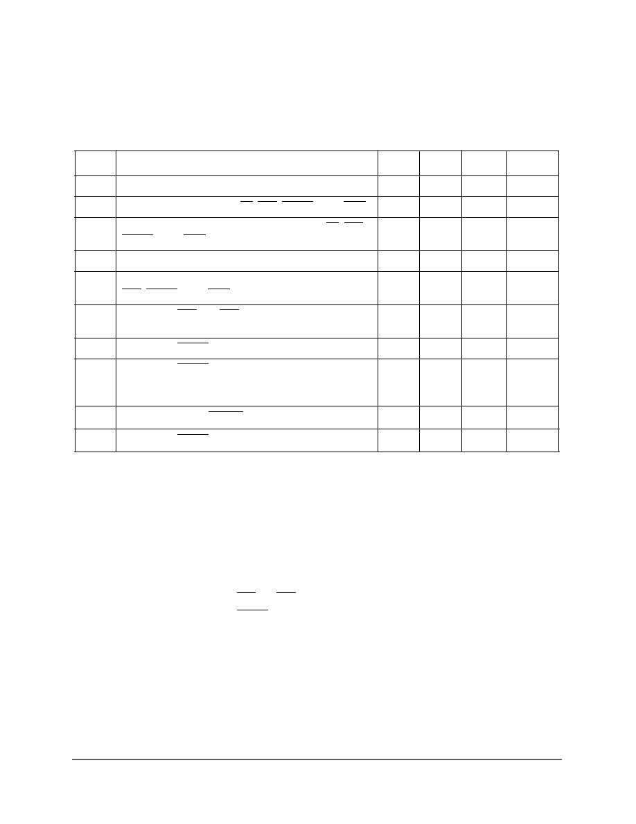
3.1.2.3 60x Bus Output AC Specications
Table 9 provides the 60x bus output AC timing specications for the PPC740 and
PPC750 as dened in Figure 5 . Output timing specication for the L2 bus are provided
Notes:
1. All output specications are measured from the 1.4 V of the rising edge of SYSCLK to the TTL level
(0.8 V or 2.0 V) of the signal in question. Both input and output timings are measured at the pin.
2. All maximum timing specications assume CL = 50 pF.
3. This minimum parameter assumes CL = 0 pF.
4. tsysclk is the period of the external bus clock (SYSCLK) in nanoseconds (ns). The numbers given in the
table must be multiplied by the period of SYSCLK to compute the actual time duration of the parame-
ter in question.
5. Output signal transitions from GND to 2.0 V or OVdd to 0.8 V.
6. Nominal precharge width for ABB and DBB is 0.5 tsysclk.
7. Nominal precharge width for ARTRY is 1.0 tsysclk.
8. Guaranteed by design and characterization, and not tested.
Table 9. 60X Bus Output AC Timing Specications1
Operating conditions are specied in Section Table 2., "Recommended Operating Conditions" CL = 50 pF
2
Num
Characteristic
Min
Max
Unit
Notes
12
SYSCLK to Output Driven (Output Enable Time)
0.5
—
ns
13
SYSCLK to Output Valid (TS, ABB, ARTRY, and DBB)
—
6.5
ns
5
14
SYSCLK to all other Output Valid (all except TS, ABB,
ARTRY
, and DBB)
—
6.5
ns
5
15
SYSCLK to Output Invalid (Output Hold)
1.0
—
ns
3
16
SYSCLK to Output High Impedance (all signals except
ABB
, ARTRY, and DBB)
—
6.0
ns
8
17
SYSCLK to ABB and DBB high impedance after pre-
charge
—
1.0
tsysclk
4,6,8
18
SYSCLK to ARTRY high impedance before precharge
—
5.5
ns
8
19
SYSCLK to ARTRY precharge enable
0.2*
tsysclk
+ 1.0
—
ns
3,4,7
20
Maximum delay to ARTRY precharge
—
1
tsysclk
4,7
21
SYSCLK to ARTRY high impedance after precharge
—
2
tsysclk
4,7,8
相关PDF资料 |
PDF描述 |
|---|---|
| ICS2494AM-XXX | 135 MHz, VIDEO CLOCK GENERATOR, PDSO20 |
| ICS650R-14IT | 133.33 MHz, OTHER CLOCK GENERATOR, PDSO20 |
| ICS650R-14T | 133.33 MHz, OTHER CLOCK GENERATOR, PDSO20 |
| ICS840001AKI-34LF | 213.33 MHz, OTHER CLOCK GENERATOR, QCC16 |
| I2041AG-8TR | 40.4 MHz, OTHER CLOCK GENERATOR, PDSO8 |
相关代理商/技术参数 |
参数描述 |
|---|---|
| IBM25EMPPC750LEBA300 | 制造商:未知厂家 制造商全称:未知厂家 功能描述:32-Bit Microprocessor |
| IBM25EMPPC750LEBA333 | 制造商:未知厂家 制造商全称:未知厂家 功能描述:32-Bit Microprocessor |
| IBM25EMPPC750LEBA366 | 制造商:未知厂家 制造商全称:未知厂家 功能描述:32-Bit Microprocessor |
| IBM25EMPPC750LEBA400 | 制造商:未知厂家 制造商全称:未知厂家 功能描述:32-Bit Microprocessor |
| IBM25EMPPC750LEBA466 | 制造商:未知厂家 制造商全称:未知厂家 功能描述:32-Bit Microprocessor |
发布紧急采购,3分钟左右您将得到回复。