参数资料
| 型号: | ISL6324IRZ-T |
| 厂商: | Intersil |
| 文件页数: | 23/38页 |
| 文件大小: | 0K |
| 描述: | IC HYBRID CTRLR PWM DUAL 48-QFN |
| 标准包装: | 4,000 |
| 应用: | 控制器,AMD SVI |
| 输入电压: | 5 V ~ 12 V |
| 输出数: | 2 |
| 输出电压: | 最高 2V |
| 工作温度: | -40°C ~ 85°C |
| 安装类型: | 表面贴装 |
| 封装/外壳: | 48-VFQFN 裸露焊盘 |
| 供应商设备封装: | 48-QFN(7x7) |
| 包装: | 带卷 (TR) |
第1页第2页第3页第4页第5页第6页第7页第8页第9页第10页第11页第12页第13页第14页第15页第16页第17页第18页第19页第20页第21页第22页当前第23页第24页第25页第26页第27页第28页第29页第30页第31页第32页第33页第34页第35页第36页第37页第38页
�� �
�
�ISL6324�
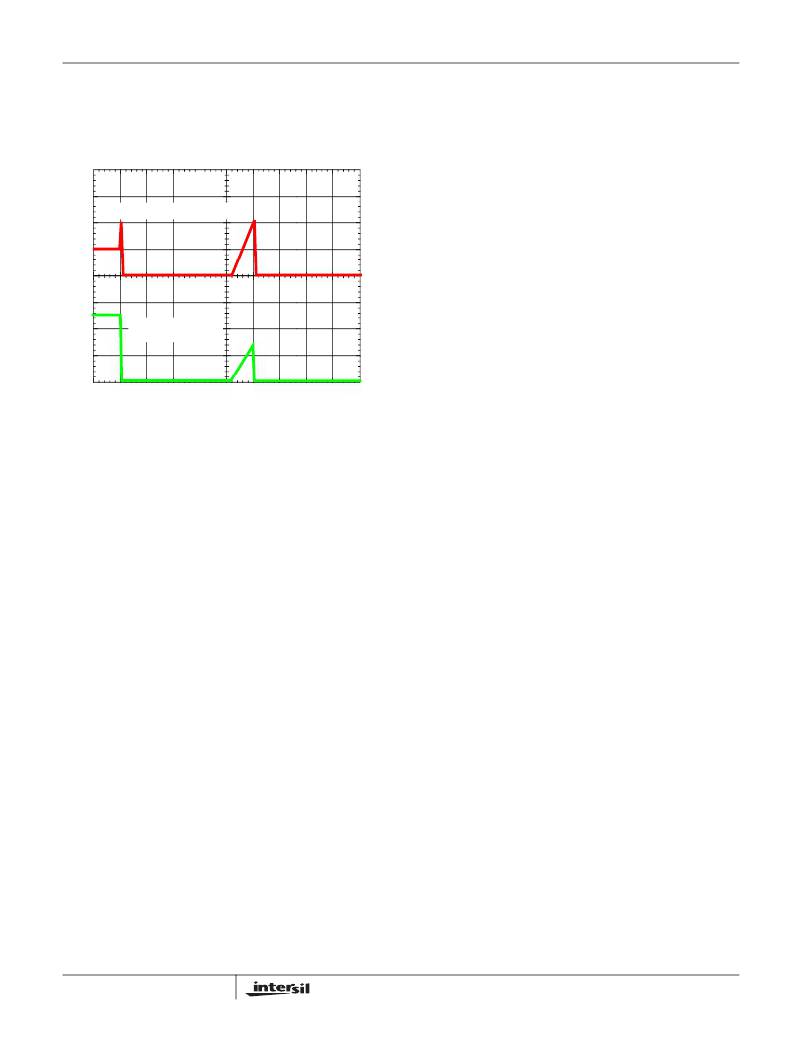
�overcurrent� shutdown� will� be� initiated.� This� will� result� in� a�
�continuous� hiccup� mode.�
�Note� that� the� energy� delivered� during� trip-retry� cycling� is�
�much� less� than� during� full-load� operation,� so� there� is� no�
�thermal� hazard.�
�OUTPUT� CURRENT,� 50A/DIV�
�0A�
�OUTPUT� VOLTAGE,�
�500mV/DIV�
�0V�
�3ms/DIV�
�FIGURE� 14.� OVERCURRENT� BEHAVIOR� IN� HICCUP� MODE�
�NORTH� BRIDGE� REGULATOR� OVERCURRENT�
�The� overcurrent� shutdown� sequence� for� the� North� Bridge�
�regulator� is� identical� to� the� Core� regulator� with� the� exception�
�that� it� is� a� single� phase� regulator� and� will� only� disable� the�
�MOSFET� drivers� for� the� North� Bridge.� Once� 7� retry� attempts�
�have� been� executed� unsuccessfully,� the� controller� will� disable�
�UGATE� and� LGATE� signals� for� both� Core� and� North� Bridge�
�and� will� latch� off� requiring� a� POR� of� VCC� to� reset� the� ISL6324.�
�Note� that� the� energy� delivered� during� trip-retry� cycling� is�
�much� less� than� during� full-load� operation,� so� there� is� no�
�thermal� hazard.�
�Individual� Channel� Overcurrent� Limiting�
�The� ISL6324� has� the� ability� to� limit� the� current� in� each�
�individual� channel� of� the� Core� regulator� without� shutting�
�down� the� entire� regulator.� This� is� accomplished� by�
�continuously� comparing� the� sensed� currents� of� each� channel�
�with� a� constant� 140μA� OCL� reference� current.� If� a� channel’s�
�individual� sensed� current� exceeds� this� OCL� limit,� the� UGATE�
�signal� of� that� channel� is� immediately� forced� low,� and� the�
�LGATE� signal� is� forced� high.� This� turns� off� the� upper�
�MOSFET(s),� turns� on� the� lower� MOSFET(s),� and� stops� the�
�rise� of� current� in� that� channel,� forcing� the� current� in� the�
�channel� to� decrease.� That� channel’s� UGATE� signal� will� not�
�be� able� to� return� high� until� the� sensed� channel� current� falls�
�back� below� the� 140μA� reference.�
�Exclusive� Operation� in� Parallel� Mode�
�The� ISL6324� was� designed� such� that� the� processor� would�
�be� the� determining� factor� of� whether� the� ISL6324� operated�
�in� PVI� mode� or� in� SVI� mode.� If,� however,� the� ISL6324� is� to�
�be� used� in� a� system� that� will� be� used� exclusively� in� parallel�
�mode� and� the� North� Bridge� regulator� will� not� be� populated� at�
�23�
�all,� there� are� some� pin� connections� that� must� be� made� in�
�order� for� the� ISL6324� to� function� properly.� The� ISEN_NB+�
�(pin� 2)� and� ISEN_NB-� (pin� 47)� pins� must� be� tied� to� ground.� A�
�small� trace� from� the� pin� to� the� ground� pad� under� the� part� is�
�all� that� is� required.� The� PVCC_NB� pin� (pin� 42)� should� be� tied�
�to� either� +5V� or� to� +12V� with� a� small� decoupling� capacitor� to�
�ground.� All� other� pins� associated� with� the� North� Bridge�
�regulator� may� be� left� unconnected.�
�I� 2� C� Bus� Interface�
�The� ISL6324� includes� an� I� 2� C� bus� interface� which� allows� for�
�user� programmability� of� three� of� the� controller� ’s� operating�
�parameters.� The� operating� parameters� that� can� be� adjusted�
�through� the� I� 2� C� are:�
�1.� Voltage� Margining� Offset� :� The� DAC� voltage� can� be�
�offset� in� 25mV� increments.�
�2.� VDDPWRGD� Trip� Level� :� The� PGOOD� trip� level� for� either�
�the� Core� regulator� or� the� North� Bridge� regulator� can� be�
�increased.�
�3.� Overvoltage� Trip� Level� :� The� OVP� trip� level� of� either� the�
�Core� or� North� Bridge� regulator� can� be� increased.�
�To� adjust� these� three� parameters,� data� transmission� from� the�
�main� microprocessor� to� the� ISL6324� and� vice� versa� must� take�
�place� through� the� two� wire� I� 2� C� bus� interface.� The� two� wires� of�
�the� I� 2� C� bus� consist� of� the� SDA� line,� over� which� all� data� is� sent,�
�and� the� SCL� line,� which� is� a� clock� signal� used� to� synchronize�
�sending/receiving� of� the� data.�
�Both� SDA� and� SCL� are� bidirectional� lines,� externally� connected�
�to� a� positive� supply� voltage� via� a� pull-up� resistor.� Pull-up�
�resistor� values� should� be� chosen� to� limit� the� input� current� to�
�less� then� 3mA� .� When� the� bus� is� free,� both� lines� are� HIGH.� The�
�output� stages� of� ISL6324� have� an� open� drain/open� collector� in�
�order� to� perform� the� wired-AND� function.� Data� on� the� I� 2� C� bus�
�can� be� transferred� up� to� 100Kbps� in� the� standard-mode� or� up� to�
�400Kbps� in� the� fast-mode.� The� level� of� logic� “0”� and� logic� “1”� is�
�dependent� on� associated� value� of� V� DD� as� per� electrical�
�specification� table.� One� clock� pulse� is� generated� for� each� data�
�bit� transferred.� The� ISL6324� is� a� “SLAVE� only”� device,� so� the�
�SCL� line� must� always� be� controlled� by� an� external� master.�
�It� is� important� to� note� that� the� I� 2� C� bus� of� the� ISL6324� only�
�works� once� the� voltage� on� the� VCC� pin� has� risen� above� the�
�POR� rising� threshold.� The� I� 2� C� will� continue� to� remain� active�
�until� the� voltage� on� the� VCC� pin� falls� back� below� the� falling�
�POR� threshold� level.�
�Data� Validity�
�The� data� on� the� SDA� line� must� be� stable� during� the� HIGH�
�period� of� the� SCL,� unless� generating� a� START� or� STOP�
�condition.� The� HIGH� or� LOW� state� of� the� data� line� can� only�
�change� when� the� clock� signal� on� the� SCL� line� is� LOW.� Refer�
�to� Figure� 15.�
�FN6518.2�
�September� 25,� 2008�
�相关PDF资料 |
PDF描述 |
|---|---|
| LT1963AET-3.3#PBF | IC REG LDO 3.3V 1.5A TO220-5 |
| HIP6004BCVZA-T | IC CTRLR PWM VOLTAGE MON 20TSSOP |
| RYM28DTMT-S189 | CONN EDGECARD 56POS R/A .156 SLD |
| GBB65DHNR | CONN EDGECARD 130PS .050 DIP SLD |
| GBB65DHHR | CONN EDGECARD 130PS .050 DIP SLD |
相关代理商/技术参数 |
参数描述 |
|---|---|
| ISL6326AIRZ | 制造商:Rochester Electronics LLC 功能描述: 制造商:Intersil Corporation 功能描述: |
| ISL6326BCRZ | 功能描述:电流型 PWM 控制器 W/ANNEAL 4-PHS VR11 CNTRLR COM RoHS:否 制造商:Texas Instruments 开关频率:27 KHz 上升时间: 下降时间: 工作电源电压:6 V to 15 V 工作电源电流:1.5 mA 输出端数量:1 最大工作温度:+ 105 C 安装风格:SMD/SMT 封装 / 箱体:TSSOP-14 |
| ISL6326BCRZ-T | 功能描述:电流型 PWM 控制器 W/ANNEAL 4-PHS VR11 CNTRLR COM RoHS:否 制造商:Texas Instruments 开关频率:27 KHz 上升时间: 下降时间: 工作电源电压:6 V to 15 V 工作电源电流:1.5 mA 输出端数量:1 最大工作温度:+ 105 C 安装风格:SMD/SMT 封装 / 箱体:TSSOP-14 |
| ISL6326BIRZ | 功能描述:电流型 PWM 控制器 W/ANNEAL 4-PHS VR11 CNTRLR IND RoHS:否 制造商:Texas Instruments 开关频率:27 KHz 上升时间: 下降时间: 工作电源电压:6 V to 15 V 工作电源电流:1.5 mA 输出端数量:1 最大工作温度:+ 105 C 安装风格:SMD/SMT 封装 / 箱体:TSSOP-14 |
| ISL6326BIRZ-T | 功能描述:电流型 PWM 控制器 W/ANNEAL 4-PHS VR11 CNTRLR IND RoHS:否 制造商:Texas Instruments 开关频率:27 KHz 上升时间: 下降时间: 工作电源电压:6 V to 15 V 工作电源电流:1.5 mA 输出端数量:1 最大工作温度:+ 105 C 安装风格:SMD/SMT 封装 / 箱体:TSSOP-14 |
发布紧急采购,3分钟左右您将得到回复。