- 您现在的位置:买卖IC网 > PDF目录299403 > LFXP2-17E-7F484C (LATTICE SEMICONDUCTOR CORP) PDF资料下载
参数资料
| 型号: | LFXP2-17E-7F484C |
| 厂商: | LATTICE SEMICONDUCTOR CORP |
| 元件分类: | FPGA |
| 中文描述: | FPGA, 420 MHz, PBGA484 |
| 封装: | 23 X 23 MM, FPBGA-484 |
| 文件页数: | 25/92页 |
| 文件大小: | 1701K |
| 代理商: | LFXP2-17E-7F484C |
第1页第2页第3页第4页第5页第6页第7页第8页第9页第10页第11页第12页第13页第14页第15页第16页第17页第18页第19页第20页第21页第22页第23页第24页当前第25页第26页第27页第28页第29页第30页第31页第32页第33页第34页第35页第36页第37页第38页第39页第40页第41页第42页第43页第44页第45页第46页第47页第48页第49页第50页第51页第52页第53页第54页第55页第56页第57页第58页第59页第60页第61页第62页第63页第64页第65页第66页第67页第68页第69页第70页第71页第72页第73页第74页第75页第76页第77页第78页第79页第80页第81页第82页第83页第84页第85页第86页第87页第88页第89页第90页第91页第92页
2-28
Architecture
Lattice Semiconductor
LatticeXP2 Family Data Sheet
The signal DDRCLKPOL controls the polarity of the clock used in the synchronization registers. It ensures ade-
quate timing when data is transferred from the DQS to system clock domain. For further discussion on this topic,
see the DDR Memory section of this data sheet.
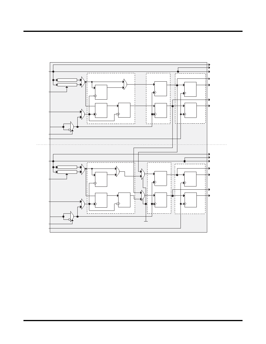
Figure 2-26. Input Register Block
Output Register Block
The output register block provides the ability to register signals from the core of the device before they are passed
to the sysIO buffers. The blocks on the PIOs on the left, right and bottom contain registers for SDR operation that
are combined with an additional latch for DDR operation. Figure 2-27 shows the diagram of the Output Register
Block for PIOs.
In SDR mode, ONEG0 feeds one of the flip-flops that then feeds the output. The flip-flop can be configured as a D-
type or latch. In DDR mode, ONEG0 and OPOS0 are fed into registers on the positive edge of the clock. At the next
clock cycle the registered OPOS0 is latched. A multiplexer running off the same clock cycle selects the correct reg-
ister to feed the output (D0).
By combining output blocks of the complementary PIOs and sharing some registers from input blocks, a gearbox
function can be implemented, to take four data streams ONEG0A, ONEG1A, ONEG1B and ONEG1B. Figure 2-27
Clock Transfer Registers
SDR & Sync
Registers
D1
D2
D0
DDR Registers
D
Q
D-Type
D
Q
D-Type
D
Q
D-Type
D
Q
D-Type
/LATCH
D
Q
D-Type
0
1
D
Q
D
Q
0
1
Fixed Delay
Dynamic Delay
DI
(From sysIO
Buffer)
DI
(From sysIO
Buffer)
INCK2
INDD
IPOS0A
QPOS0A
IPOS1A
QPOS1A
DEL [3:0]
CLK0 (of PIO A)
Delayed
DQS
0
1
CLKA
DQ
D
Q
D
Q
0
1
0
1
D
Q
D
Q
0
1
D
Q
D
Q
0
1
Fixed Delay
Dynamic Delay
INCK2
INDD
IPOS0B
QPOS0B
IPOS1B
QPOS1B
DEL [3:0]
CLK0 (of PIO B)
Delayed
DQS
CLKB
/LATCH
True PIO (A) in LVDS I/O Pair
Comp PIO (B) in LVDS I/O Pair
D-Type1
D-Type
/LATCH
D-Type
/LATCH
D-Type1
From
Routing
To
Routing
D1
D2
D0
DDR Registers
SDR & Sync
Registers
0
1
DDRSRC
Gearbox Configuration Bit
DDRCLKPOL
1. Shared with output register
2. Selected PIO.
Note: Simplified version does not
show CE and SET/RESET details
From
Routing
To
Routing
To DQS Delay Block2
D-Type
相关PDF资料 |
PDF描述 |
|---|---|
| LFXP20E-3FN484C | |
| LFXP20E-5FN484C | |
| LFXP15C-4FN256C | |
| LFZ3508VXX | GENERAL PURPOSE INDUCTOR |
| LFZ2805HXX | GENERAL PURPOSE INDUCTOR |
相关代理商/技术参数 |
参数描述 |
|---|---|
| LFXP2-17E-7F484C8W | 功能描述:FPGA - 现场可编程门阵列 17KLUTs 358I/O Inst- on DSP 1.2V -7Spd RoHS:否 制造商:Altera Corporation 系列:Cyclone V E 栅极数量: 逻辑块数量:943 内嵌式块RAM - EBR:1956 kbit 输入/输出端数量:128 最大工作频率:800 MHz 工作电源电压:1.1 V 最大工作温度:+ 70 C 安装风格:SMD/SMT 封装 / 箱体:FBGA-256 |
| LFXP2-17E-7FN484C | 功能描述:FPGA - 现场可编程门阵列 17KLUTs 358 I/O Inst -on DSP 1.2V -6 Spd RoHS:否 制造商:Altera Corporation 系列:Cyclone V E 栅极数量: 逻辑块数量:943 内嵌式块RAM - EBR:1956 kbit 输入/输出端数量:128 最大工作频率:800 MHz 工作电源电压:1.1 V 最大工作温度:+ 70 C 安装风格:SMD/SMT 封装 / 箱体:FBGA-256 |
| LFXP2-17E-7FN484C8W | 功能描述:FPGA - 现场可编程门阵列 17KLUTs 358I/O Inst -on DSP 1.2V -7 Spd RoHS:否 制造商:Altera Corporation 系列:Cyclone V E 栅极数量: 逻辑块数量:943 内嵌式块RAM - EBR:1956 kbit 输入/输出端数量:128 最大工作频率:800 MHz 工作电源电压:1.1 V 最大工作温度:+ 70 C 安装风格:SMD/SMT 封装 / 箱体:FBGA-256 |
| LFXP2-17E-7FT256C | 功能描述:FPGA - 现场可编程门阵列 17KLUTs 201 I/O Inst -on DSP 1.2V -7 Spd RoHS:否 制造商:Altera Corporation 系列:Cyclone V E 栅极数量: 逻辑块数量:943 内嵌式块RAM - EBR:1956 kbit 输入/输出端数量:128 最大工作频率:800 MHz 工作电源电压:1.1 V 最大工作温度:+ 70 C 安装风格:SMD/SMT 封装 / 箱体:FBGA-256 |
| LFXP2-17E-7FT256C8W | 功能描述:FPGA - 现场可编程门阵列 17KLUTs 201 I/O Inst -on DSP 1.2V -7 Spd RoHS:否 制造商:Altera Corporation 系列:Cyclone V E 栅极数量: 逻辑块数量:943 内嵌式块RAM - EBR:1956 kbit 输入/输出端数量:128 最大工作频率:800 MHz 工作电源电压:1.1 V 最大工作温度:+ 70 C 安装风格:SMD/SMT 封装 / 箱体:FBGA-256 |
发布紧急采购,3分钟左右您将得到回复。