- 您现在的位置:买卖IC网 > PDF目录299403 > LFXP2-17E-7F484C (LATTICE SEMICONDUCTOR CORP) PDF资料下载
参数资料
| 型号: | LFXP2-17E-7F484C |
| 厂商: | LATTICE SEMICONDUCTOR CORP |
| 元件分类: | FPGA |
| 中文描述: | FPGA, 420 MHz, PBGA484 |
| 封装: | 23 X 23 MM, FPBGA-484 |
| 文件页数: | 48/92页 |
| 文件大小: | 1701K |
| 代理商: | LFXP2-17E-7F484C |
第1页第2页第3页第4页第5页第6页第7页第8页第9页第10页第11页第12页第13页第14页第15页第16页第17页第18页第19页第20页第21页第22页第23页第24页第25页第26页第27页第28页第29页第30页第31页第32页第33页第34页第35页第36页第37页第38页第39页第40页第41页第42页第43页第44页第45页第46页第47页当前第48页第49页第50页第51页第52页第53页第54页第55页第56页第57页第58页第59页第60页第61页第62页第63页第64页第65页第66页第67页第68页第69页第70页第71页第72页第73页第74页第75页第76页第77页第78页第79页第80页第81页第82页第83页第84页第85页第86页第87页第88页第89页第90页第91页第92页
3-8
DC and Switching Characteristics
Lattice Semiconductor
LatticeXP2 Family Data Sheet
sysIO Differential Electrical Characteristics
LVDS
Over Recommended Operating Conditions
Differential HSTL and SSTL
Differential HSTL and SSTL outputs are implemented as a pair of complementary single-ended outputs. All allow-
able single-ended output classes (class I and class II) are supported in this mode.
For further information on LVPECL, RSDS, MLVDS, BLVDS and other differential interfaces please see details in
additional technical notes listed at the end of this data sheet.
LVDS25E
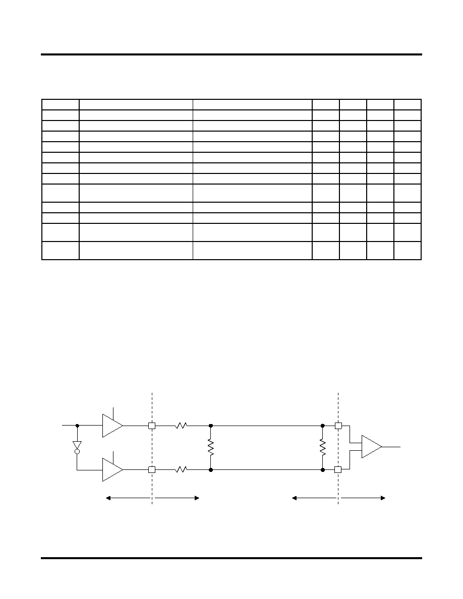
The top and bottom sides of LatticeXP2 devices support LVDS outputs via emulated complementary LVCMOS out-
puts in conjunction with a parallel resistor across the driver outputs. The scheme shown in Figure 3-1 is one possi-
ble solution for point-to-point signals.
Figure 3-1. LVDS25E Output Termination Example
Parameter
Description
Test Conditions
Min.
Typ.
Max.
Units
VINP, VINM Input Voltage
0
—
2.4
V
VCM
Input Common Mode Voltage
Half the Sum of the Two Inputs
0.05
—
2.35
V
VTHD
Differential Input Threshold
Difference Between the Two Inputs
+/-100
—
mV
IIN
Input Current
Power On or Power Off
—
+/-10
A
VOH
Output High Voltage for VOP or VOM RT = 100 Ohm
—
1.38
1.60
V
VOL
Output Low Voltage for VOP or VOM
RT = 100 Ohm
0.9V
1.03
—
V
VOD
Output Voltage Differential
(VOP - VOM), RT = 100 Ohm
250
350
450
mV
V
OD
Change in VOD Between High and
Low
——
50
mV
VOS
Output Voltage Offset
(VOP + VOM)/2, RT = 100 Ohm
1.125
1.20
1.375
V
OS
Change in VOS Between H and L
—
50
mV
ISA
Output Short Circuit Current
VOD = 0V Driver Outputs Shorted to
Ground
——
24
mA
ISAB
Output Short Circuit Current
VOD = 0V Driver Outputs Shorted to
Each Other
——
12
mA
+
-
RS=158 ohms
(±1%)
RS=158 ohms
(±1%)
RP = 140 ohms
(±1%)
RT = 100 ohms
(±1%)
OFF-chip
Transmission line, Zo = 100 ohm differential
VCCIO = 2.5V (±5%)
8 mA
VCCIO = 2.5V (±5%)
ON-chip
OFF-chip ON-chip
8 mA
相关PDF资料 |
PDF描述 |
|---|---|
| LFXP20E-3FN484C | |
| LFXP20E-5FN484C | |
| LFXP15C-4FN256C | |
| LFZ3508VXX | GENERAL PURPOSE INDUCTOR |
| LFZ2805HXX | GENERAL PURPOSE INDUCTOR |
相关代理商/技术参数 |
参数描述 |
|---|---|
| LFXP2-17E-7F484C8W | 功能描述:FPGA - 现场可编程门阵列 17KLUTs 358I/O Inst- on DSP 1.2V -7Spd RoHS:否 制造商:Altera Corporation 系列:Cyclone V E 栅极数量: 逻辑块数量:943 内嵌式块RAM - EBR:1956 kbit 输入/输出端数量:128 最大工作频率:800 MHz 工作电源电压:1.1 V 最大工作温度:+ 70 C 安装风格:SMD/SMT 封装 / 箱体:FBGA-256 |
| LFXP2-17E-7FN484C | 功能描述:FPGA - 现场可编程门阵列 17KLUTs 358 I/O Inst -on DSP 1.2V -6 Spd RoHS:否 制造商:Altera Corporation 系列:Cyclone V E 栅极数量: 逻辑块数量:943 内嵌式块RAM - EBR:1956 kbit 输入/输出端数量:128 最大工作频率:800 MHz 工作电源电压:1.1 V 最大工作温度:+ 70 C 安装风格:SMD/SMT 封装 / 箱体:FBGA-256 |
| LFXP2-17E-7FN484C8W | 功能描述:FPGA - 现场可编程门阵列 17KLUTs 358I/O Inst -on DSP 1.2V -7 Spd RoHS:否 制造商:Altera Corporation 系列:Cyclone V E 栅极数量: 逻辑块数量:943 内嵌式块RAM - EBR:1956 kbit 输入/输出端数量:128 最大工作频率:800 MHz 工作电源电压:1.1 V 最大工作温度:+ 70 C 安装风格:SMD/SMT 封装 / 箱体:FBGA-256 |
| LFXP2-17E-7FT256C | 功能描述:FPGA - 现场可编程门阵列 17KLUTs 201 I/O Inst -on DSP 1.2V -7 Spd RoHS:否 制造商:Altera Corporation 系列:Cyclone V E 栅极数量: 逻辑块数量:943 内嵌式块RAM - EBR:1956 kbit 输入/输出端数量:128 最大工作频率:800 MHz 工作电源电压:1.1 V 最大工作温度:+ 70 C 安装风格:SMD/SMT 封装 / 箱体:FBGA-256 |
| LFXP2-17E-7FT256C8W | 功能描述:FPGA - 现场可编程门阵列 17KLUTs 201 I/O Inst -on DSP 1.2V -7 Spd RoHS:否 制造商:Altera Corporation 系列:Cyclone V E 栅极数量: 逻辑块数量:943 内嵌式块RAM - EBR:1956 kbit 输入/输出端数量:128 最大工作频率:800 MHz 工作电源电压:1.1 V 最大工作温度:+ 70 C 安装风格:SMD/SMT 封装 / 箱体:FBGA-256 |
发布紧急采购,3分钟左右您将得到回复。