- 您现在的位置:买卖IC网 > PDF目录299403 > LFXP2-17E-7F484C (LATTICE SEMICONDUCTOR CORP) PDF资料下载
参数资料
| 型号: | LFXP2-17E-7F484C |
| 厂商: | LATTICE SEMICONDUCTOR CORP |
| 元件分类: | FPGA |
| 中文描述: | FPGA, 420 MHz, PBGA484 |
| 封装: | 23 X 23 MM, FPBGA-484 |
| 文件页数: | 36/92页 |
| 文件大小: | 1701K |
| 代理商: | LFXP2-17E-7F484C |
第1页第2页第3页第4页第5页第6页第7页第8页第9页第10页第11页第12页第13页第14页第15页第16页第17页第18页第19页第20页第21页第22页第23页第24页第25页第26页第27页第28页第29页第30页第31页第32页第33页第34页第35页当前第36页第37页第38页第39页第40页第41页第42页第43页第44页第45页第46页第47页第48页第49页第50页第51页第52页第53页第54页第55页第56页第57页第58页第59页第60页第61页第62页第63页第64页第65页第66页第67页第68页第69页第70页第71页第72页第73页第74页第75页第76页第77页第78页第79页第80页第81页第82页第83页第84页第85页第86页第87页第88页第89页第90页第91页第92页
2-38
Architecture
Lattice Semiconductor
LatticeXP2 Family Data Sheet
and loaded directly onto test nodes, or test data to be captured and shifted out for veri cation. The test access port
consists of dedicated I/Os: TDI, TDO, TCK and TMS. The test access port has its own supply voltage VCCJ and can
operate with LVCMOS3.3, 2.5, 1.8, 1.5 and 1.2 standards. For more information, please see TN1141, LatticeXP2
flexiFLASH Device Configuration
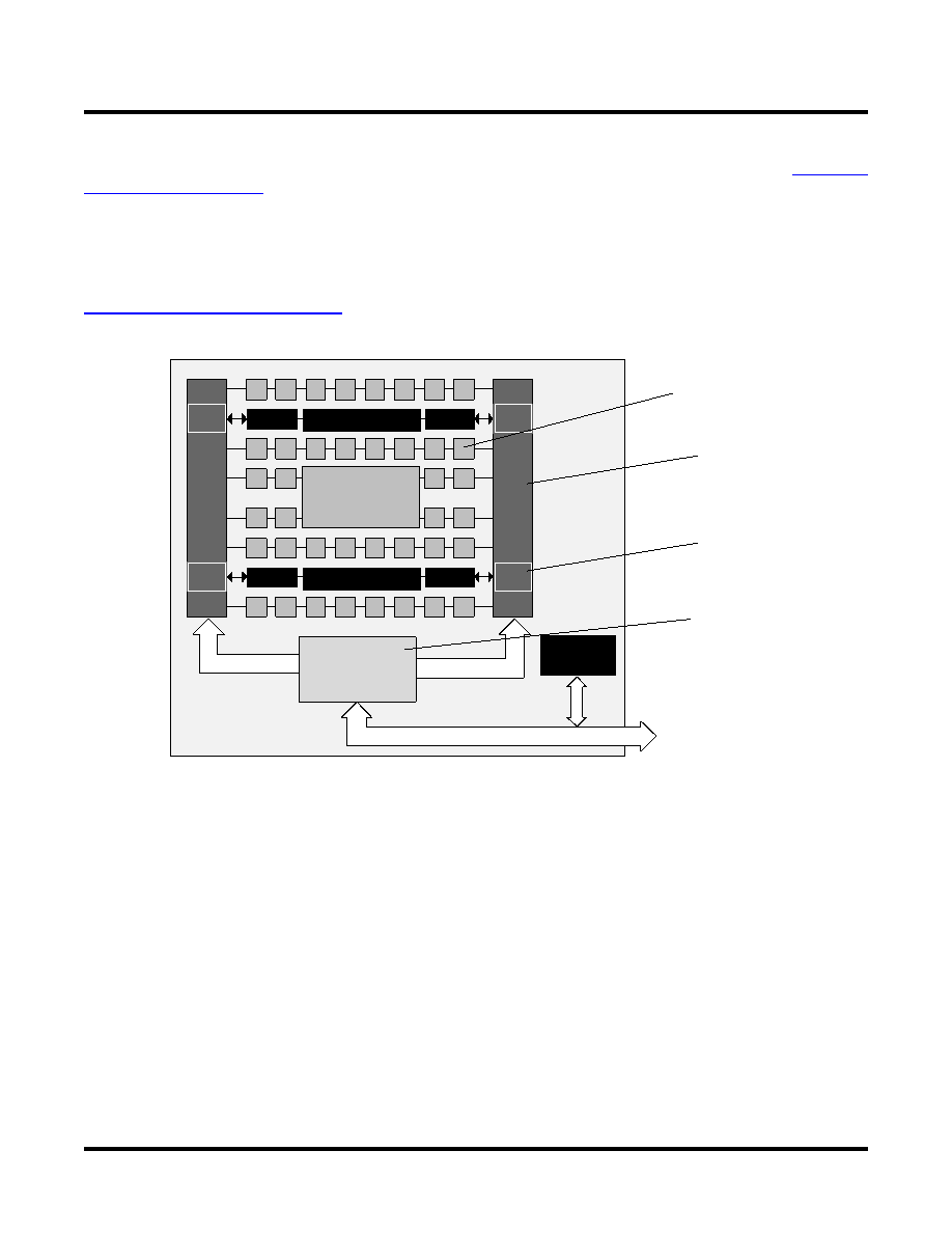
The LatticeXP2 devices combine Flash and SRAM on a single chip to provide users with flexibility in device pro-
gramming and configuration. Figure 2-33 provides an overview of the arrangement of Flash and SRAM configura-
tion cells within the device. The remainder of this section provides an overview of these capabilities. See TN1141,
LatticeXP2 sysCONFIG Usage Guide for a more detailed description.
Figure 2-33. Overview of Flash and SRAM Configuration Cells Within LatticeXP2 Devices
At power-up, or on user command, data is transferred from the on-chip Flash memory to the SRAM configuration
cells that control the operation of the device. This is done with massively parallel buses enabling the parts to oper-
ate within microseconds of the power supplies reaching valid levels; this capability is referred to as Instant-On.
The on-chip Flash enables a single-chip solution eliminating the need for external boot memory. This Flash can be
programmed through either the JTAG or Slave SPI ports of the device. The SRAM configuration space can also be
infinitely reconfigured through the JTAG and Master SPI ports. The JTAG port is IEEE 1149.1 and IEEE 1532 com-
pliant.
As described in the EBR section of the data sheet, the FlashBAK capability of the parts enables the contents of the
EBR blocks to be written back into the Flash storage area without erasing or reprogramming other aspects of the
device configuration. Serial TAG memory is also available to allow the storage of small amounts of data such as
calibration coefficients and error codes.
For applications where security is important, the lack of an external bitstream provides a solution that is inherently
more secure than SRAM only FPGAs. This is further enhanced by device locking. The device can be in one of
three modes:
EBR Blocks
Flash
Memory
EBR Blocks
SRAM
Configuration
Bits
Massively Parallel
Data Transfer
Instant-ON
Flash for
Single-Chip
Solution
FlashBAK
for EBR
Storage
Decryption
and Device
Lock
SPI and JTAG
TAG
Memory
Device Lock
for Design
Security
相关PDF资料 |
PDF描述 |
|---|---|
| LFXP20E-3FN484C | |
| LFXP20E-5FN484C | |
| LFXP15C-4FN256C | |
| LFZ3508VXX | GENERAL PURPOSE INDUCTOR |
| LFZ2805HXX | GENERAL PURPOSE INDUCTOR |
相关代理商/技术参数 |
参数描述 |
|---|---|
| LFXP2-17E-7F484C8W | 功能描述:FPGA - 现场可编程门阵列 17KLUTs 358I/O Inst- on DSP 1.2V -7Spd RoHS:否 制造商:Altera Corporation 系列:Cyclone V E 栅极数量: 逻辑块数量:943 内嵌式块RAM - EBR:1956 kbit 输入/输出端数量:128 最大工作频率:800 MHz 工作电源电压:1.1 V 最大工作温度:+ 70 C 安装风格:SMD/SMT 封装 / 箱体:FBGA-256 |
| LFXP2-17E-7FN484C | 功能描述:FPGA - 现场可编程门阵列 17KLUTs 358 I/O Inst -on DSP 1.2V -6 Spd RoHS:否 制造商:Altera Corporation 系列:Cyclone V E 栅极数量: 逻辑块数量:943 内嵌式块RAM - EBR:1956 kbit 输入/输出端数量:128 最大工作频率:800 MHz 工作电源电压:1.1 V 最大工作温度:+ 70 C 安装风格:SMD/SMT 封装 / 箱体:FBGA-256 |
| LFXP2-17E-7FN484C8W | 功能描述:FPGA - 现场可编程门阵列 17KLUTs 358I/O Inst -on DSP 1.2V -7 Spd RoHS:否 制造商:Altera Corporation 系列:Cyclone V E 栅极数量: 逻辑块数量:943 内嵌式块RAM - EBR:1956 kbit 输入/输出端数量:128 最大工作频率:800 MHz 工作电源电压:1.1 V 最大工作温度:+ 70 C 安装风格:SMD/SMT 封装 / 箱体:FBGA-256 |
| LFXP2-17E-7FT256C | 功能描述:FPGA - 现场可编程门阵列 17KLUTs 201 I/O Inst -on DSP 1.2V -7 Spd RoHS:否 制造商:Altera Corporation 系列:Cyclone V E 栅极数量: 逻辑块数量:943 内嵌式块RAM - EBR:1956 kbit 输入/输出端数量:128 最大工作频率:800 MHz 工作电源电压:1.1 V 最大工作温度:+ 70 C 安装风格:SMD/SMT 封装 / 箱体:FBGA-256 |
| LFXP2-17E-7FT256C8W | 功能描述:FPGA - 现场可编程门阵列 17KLUTs 201 I/O Inst -on DSP 1.2V -7 Spd RoHS:否 制造商:Altera Corporation 系列:Cyclone V E 栅极数量: 逻辑块数量:943 内嵌式块RAM - EBR:1956 kbit 输入/输出端数量:128 最大工作频率:800 MHz 工作电源电压:1.1 V 最大工作温度:+ 70 C 安装风格:SMD/SMT 封装 / 箱体:FBGA-256 |
发布紧急采购,3分钟左右您将得到回复。