- 您现在的位置:买卖IC网 > PDF目录299403 > LFXP2-17E-7F484C (LATTICE SEMICONDUCTOR CORP) PDF资料下载
参数资料
| 型号: | LFXP2-17E-7F484C |
| 厂商: | LATTICE SEMICONDUCTOR CORP |
| 元件分类: | FPGA |
| 中文描述: | FPGA, 420 MHz, PBGA484 |
| 封装: | 23 X 23 MM, FPBGA-484 |
| 文件页数: | 35/92页 |
| 文件大小: | 1701K |
| 代理商: | LFXP2-17E-7F484C |
第1页第2页第3页第4页第5页第6页第7页第8页第9页第10页第11页第12页第13页第14页第15页第16页第17页第18页第19页第20页第21页第22页第23页第24页第25页第26页第27页第28页第29页第30页第31页第32页第33页第34页当前第35页第36页第37页第38页第39页第40页第41页第42页第43页第44页第45页第46页第47页第48页第49页第50页第51页第52页第53页第54页第55页第56页第57页第58页第59页第60页第61页第62页第63页第64页第65页第66页第67页第68页第69页第70页第71页第72页第73页第74页第75页第76页第77页第78页第79页第80页第81页第82页第83页第84页第85页第86页第87页第88页第89页第90页第91页第92页
2-37
Architecture
Lattice Semiconductor
LatticeXP2 Family Data Sheet
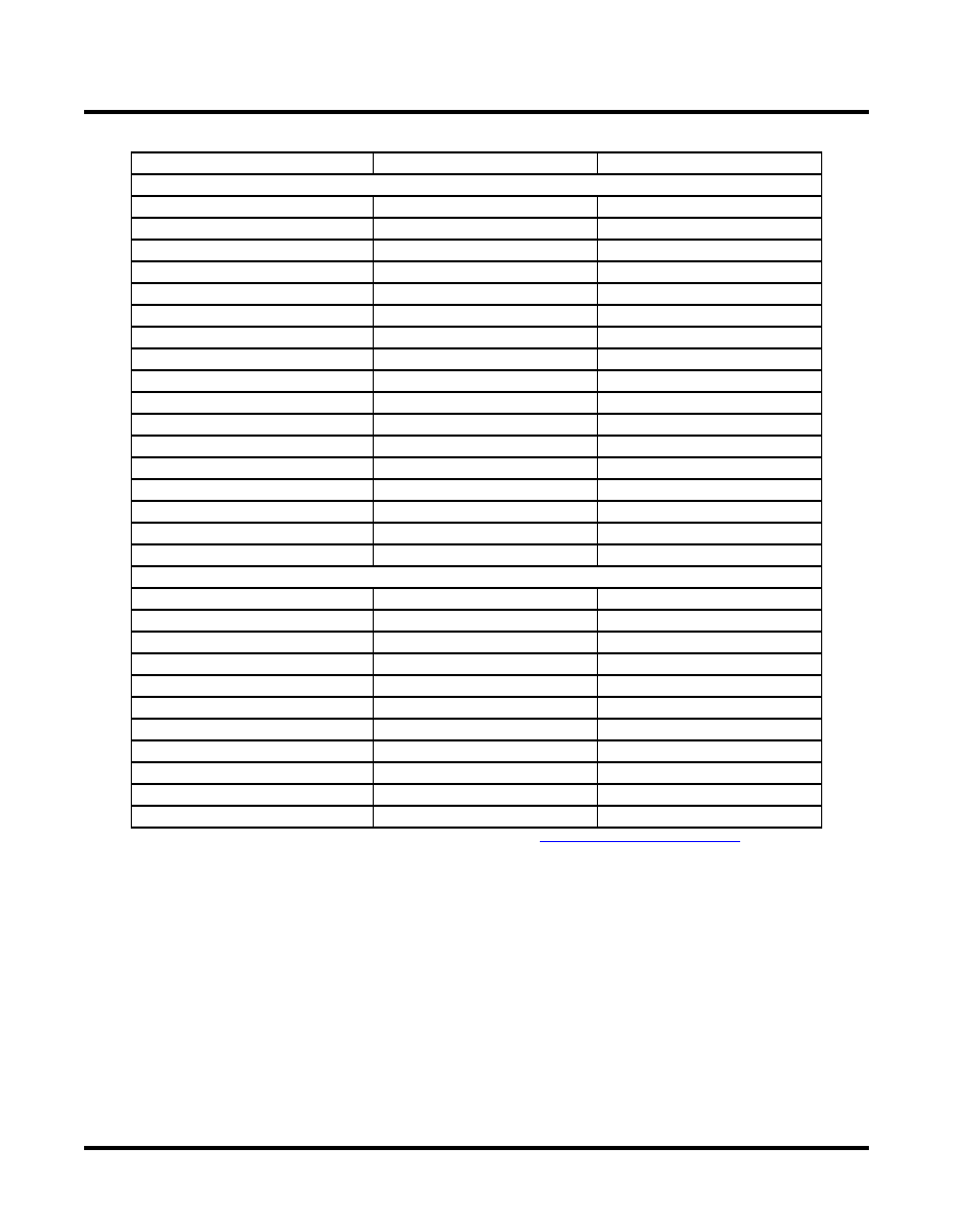
Table 2-13. Supported Output Standards
Hot Socketing
LatticeXP2 devices have been carefully designed to ensure predictable behavior during power-up and power-
down. Power supplies can be sequenced in any order. During power-up and power-down sequences, the I/Os
remain in tri-state until the power supply voltage is high enough to ensure reliable operation. In addition, leakage
into I/O pins is controlled to within specified limits. This allows for easy integration with the rest of the system.
These capabilities make the LatticeXP2 ideal for many multiple power supply and hot-swap applications.
IEEE 1149.1-Compliant Boundary Scan Testability
All LatticeXP2 devices have boundary scan cells that are accessed through an IEEE 1149.1 compliant Test Access
Port (TAP). This allows functional testing of the circuit board, on which the device is mounted, through a serial scan
path that can access all critical logic nodes. Internal registers are linked internally, allowing test data to be shifted in
Output Standard
Drive
VCCIO (Nom.)
Single-ended Interfaces
LVTTL
4mA, 8mA, 12mA, 16mA, 20mA
3.3
LVCMOS33
4mA, 8mA, 12mA 16mA, 20mA
3.3
LVCMOS25
4mA, 8mA, 12mA, 16mA, 20mA
2.5
LVCMOS18
4mA, 8mA, 12mA, 16mA
1.8
LVCMOS15
4mA, 8mA
1.5
LVCMOS12
2mA, 6mA
1.2
LVCMOS33, Open Drain
4mA, 8mA, 12mA 16mA, 20mA
—
LVCMOS25, Open Drain
4mA, 8mA, 12mA 16mA, 20mA
—
LVCMOS18, Open Drain
4mA, 8mA, 12mA 16mA
—
LVCMOS15, Open Drain
4mA, 8mA
—
LVCMOS12, Open Drain
2mA, 6mA
—
PCI33
N/A
3.3
HSTL18 Class I, II
N/A
1.8
HSTL15 Class I
N/A
1.5
SSTL33 Class I, II
N/A
3.3
SSTL25 Class I, II
N/A
2.5
SSTL18 Class I, II
N/A
1.8
Differential Interfaces
Differential SSTL33, Class I, II
N/A
3.3
Differential SSTL25, Class I, II
N/A
2.5
Differential SSTL18, Class I, II
N/A
1.8
Differential HSTL18, Class I, II
N/A
1.8
Differential HSTL15, Class I
N/A
1.5
LVDS
1, 2
N/A
2.5
MLVDS
1
N/A
2.5
BLVDS
1
N/A
2.5
LVPECL
1
N/A
3.3
RSDS
1
N/A
2.5
LVCMOS33D
1
4mA, 8mA, 12mA, 16mA, 20mA
3.3
1. Emulated with external resistors. For more detail, please see TN1138, LatticeXP2 High Speed I/O Interface.
2. On the left and right edges, LVDS outputs are supported with a dedicated differential output driver on 50% of the I/Os. This
solution does not require external resistors at the driver.
相关PDF资料 |
PDF描述 |
|---|---|
| LFXP20E-3FN484C | |
| LFXP20E-5FN484C | |
| LFXP15C-4FN256C | |
| LFZ3508VXX | GENERAL PURPOSE INDUCTOR |
| LFZ2805HXX | GENERAL PURPOSE INDUCTOR |
相关代理商/技术参数 |
参数描述 |
|---|---|
| LFXP2-17E-7F484C8W | 功能描述:FPGA - 现场可编程门阵列 17KLUTs 358I/O Inst- on DSP 1.2V -7Spd RoHS:否 制造商:Altera Corporation 系列:Cyclone V E 栅极数量: 逻辑块数量:943 内嵌式块RAM - EBR:1956 kbit 输入/输出端数量:128 最大工作频率:800 MHz 工作电源电压:1.1 V 最大工作温度:+ 70 C 安装风格:SMD/SMT 封装 / 箱体:FBGA-256 |
| LFXP2-17E-7FN484C | 功能描述:FPGA - 现场可编程门阵列 17KLUTs 358 I/O Inst -on DSP 1.2V -6 Spd RoHS:否 制造商:Altera Corporation 系列:Cyclone V E 栅极数量: 逻辑块数量:943 内嵌式块RAM - EBR:1956 kbit 输入/输出端数量:128 最大工作频率:800 MHz 工作电源电压:1.1 V 最大工作温度:+ 70 C 安装风格:SMD/SMT 封装 / 箱体:FBGA-256 |
| LFXP2-17E-7FN484C8W | 功能描述:FPGA - 现场可编程门阵列 17KLUTs 358I/O Inst -on DSP 1.2V -7 Spd RoHS:否 制造商:Altera Corporation 系列:Cyclone V E 栅极数量: 逻辑块数量:943 内嵌式块RAM - EBR:1956 kbit 输入/输出端数量:128 最大工作频率:800 MHz 工作电源电压:1.1 V 最大工作温度:+ 70 C 安装风格:SMD/SMT 封装 / 箱体:FBGA-256 |
| LFXP2-17E-7FT256C | 功能描述:FPGA - 现场可编程门阵列 17KLUTs 201 I/O Inst -on DSP 1.2V -7 Spd RoHS:否 制造商:Altera Corporation 系列:Cyclone V E 栅极数量: 逻辑块数量:943 内嵌式块RAM - EBR:1956 kbit 输入/输出端数量:128 最大工作频率:800 MHz 工作电源电压:1.1 V 最大工作温度:+ 70 C 安装风格:SMD/SMT 封装 / 箱体:FBGA-256 |
| LFXP2-17E-7FT256C8W | 功能描述:FPGA - 现场可编程门阵列 17KLUTs 201 I/O Inst -on DSP 1.2V -7 Spd RoHS:否 制造商:Altera Corporation 系列:Cyclone V E 栅极数量: 逻辑块数量:943 内嵌式块RAM - EBR:1956 kbit 输入/输出端数量:128 最大工作频率:800 MHz 工作电源电压:1.1 V 最大工作温度:+ 70 C 安装风格:SMD/SMT 封装 / 箱体:FBGA-256 |
发布紧急采购,3分钟左右您将得到回复。