- 您现在的位置:买卖IC网 > PDF目录299403 > LFXP2-17E-7F484C (LATTICE SEMICONDUCTOR CORP) PDF资料下载
参数资料
| 型号: | LFXP2-17E-7F484C |
| 厂商: | LATTICE SEMICONDUCTOR CORP |
| 元件分类: | FPGA |
| 中文描述: | FPGA, 420 MHz, PBGA484 |
| 封装: | 23 X 23 MM, FPBGA-484 |
| 文件页数: | 31/92页 |
| 文件大小: | 1701K |
| 代理商: | LFXP2-17E-7F484C |
第1页第2页第3页第4页第5页第6页第7页第8页第9页第10页第11页第12页第13页第14页第15页第16页第17页第18页第19页第20页第21页第22页第23页第24页第25页第26页第27页第28页第29页第30页当前第31页第32页第33页第34页第35页第36页第37页第38页第39页第40页第41页第42页第43页第44页第45页第46页第47页第48页第49页第50页第51页第52页第53页第54页第55页第56页第57页第58页第59页第60页第61页第62页第63页第64页第65页第66页第67页第68页第69页第70页第71页第72页第73页第74页第75页第76页第77页第78页第79页第80页第81页第82页第83页第84页第85页第86页第87页第88页第89页第90页第91页第92页
2-34
Architecture
Lattice Semiconductor
LatticeXP2 Family Data Sheet
DQSXFER
LatticeXP2 devices provide a DQSXFER signal to the output buffer to assist it in data transfer to DDR memories
that require DQS strobe be shifted 90
o. This shifted DQS strobe is generated by the DQSDEL block. The
DQSXFER signal runs the span of the data bus.
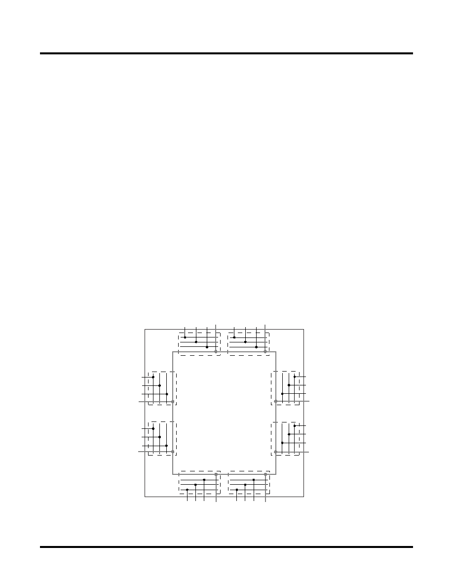
sysIO Buffer
Each I/O is associated with a exible buffer referred to as a sysIO buffer. These buffers are arranged around the
periphery of the device in groups referred to as banks. The sysIO buffers allow users to implement the wide variety
of standards that are found in today’s systems including LVCMOS, SSTL, HSTL, LVDS and LVPECL.
sysIO Buffer Banks
LatticeXP2 devices have eight sysIO buffer banks for user I/Os arranged two per side. Each bank is capable of sup-
porting multiple I/O standards. Each sysIO bank has its own I/O supply voltage (VCCIO). In addition, each bank has
voltage references, VREF1 and VREF2, that allow it to be completely independent from the others. Figure 2-32
shows the eight banks and their associated supplies.
In LatticeXP2 devices, single-ended output buffers and ratioed input buffers (LVTTL, LVCMOS and PCI) are pow-
ered using VCCIO. LVTTL, LVCMOS33, LVCMOS25 and LVCMOS12 can also be set as fixed threshold inputs inde-
pendent of VCCIO.
Each bank can support up to two separate VREF voltages, VREF1 and VREF2, that set the threshold for the refer-
enced input buffers. Some dedicated I/O pins in a bank can be configured to be a reference voltage supply pin.
Each I/O is individually configurable based on the bank’s supply and reference voltages.
Figure 2-32. LatticeXP2 Banks
VREF1(2)
GND
B
ank
2
V
CCIO2
VREF2(2)
VREF1(3)
GND
Ban
k
3
V
CCIO3
VREF2(3)
V
REF1(7)
GND
Ban
k
7
V
CCIO7
V
REF2(7)
V
REF1(6)
GND
Ban
k
6
V
CCIO6
V
REF2(6)
Bank 5
Bank 4
V
REF
1
(0
)
G
ND
Bank 0
V
CCI
O0
V
REF2(0)
V
RE
F1
(1
)
GND
Bank 1
V
CC
IO1
V
REF2(1
)
LEF
T
RIGHT
TOP
V
REF1(5
)
GND
V
CCIO5
V
REF
2(5
)
V
REF1(4)
GND
V
CCIO4
V
REF
2(4)
BOTTOM
相关PDF资料 |
PDF描述 |
|---|---|
| LFXP20E-3FN484C | |
| LFXP20E-5FN484C | |
| LFXP15C-4FN256C | |
| LFZ3508VXX | GENERAL PURPOSE INDUCTOR |
| LFZ2805HXX | GENERAL PURPOSE INDUCTOR |
相关代理商/技术参数 |
参数描述 |
|---|---|
| LFXP2-17E-7F484C8W | 功能描述:FPGA - 现场可编程门阵列 17KLUTs 358I/O Inst- on DSP 1.2V -7Spd RoHS:否 制造商:Altera Corporation 系列:Cyclone V E 栅极数量: 逻辑块数量:943 内嵌式块RAM - EBR:1956 kbit 输入/输出端数量:128 最大工作频率:800 MHz 工作电源电压:1.1 V 最大工作温度:+ 70 C 安装风格:SMD/SMT 封装 / 箱体:FBGA-256 |
| LFXP2-17E-7FN484C | 功能描述:FPGA - 现场可编程门阵列 17KLUTs 358 I/O Inst -on DSP 1.2V -6 Spd RoHS:否 制造商:Altera Corporation 系列:Cyclone V E 栅极数量: 逻辑块数量:943 内嵌式块RAM - EBR:1956 kbit 输入/输出端数量:128 最大工作频率:800 MHz 工作电源电压:1.1 V 最大工作温度:+ 70 C 安装风格:SMD/SMT 封装 / 箱体:FBGA-256 |
| LFXP2-17E-7FN484C8W | 功能描述:FPGA - 现场可编程门阵列 17KLUTs 358I/O Inst -on DSP 1.2V -7 Spd RoHS:否 制造商:Altera Corporation 系列:Cyclone V E 栅极数量: 逻辑块数量:943 内嵌式块RAM - EBR:1956 kbit 输入/输出端数量:128 最大工作频率:800 MHz 工作电源电压:1.1 V 最大工作温度:+ 70 C 安装风格:SMD/SMT 封装 / 箱体:FBGA-256 |
| LFXP2-17E-7FT256C | 功能描述:FPGA - 现场可编程门阵列 17KLUTs 201 I/O Inst -on DSP 1.2V -7 Spd RoHS:否 制造商:Altera Corporation 系列:Cyclone V E 栅极数量: 逻辑块数量:943 内嵌式块RAM - EBR:1956 kbit 输入/输出端数量:128 最大工作频率:800 MHz 工作电源电压:1.1 V 最大工作温度:+ 70 C 安装风格:SMD/SMT 封装 / 箱体:FBGA-256 |
| LFXP2-17E-7FT256C8W | 功能描述:FPGA - 现场可编程门阵列 17KLUTs 201 I/O Inst -on DSP 1.2V -7 Spd RoHS:否 制造商:Altera Corporation 系列:Cyclone V E 栅极数量: 逻辑块数量:943 内嵌式块RAM - EBR:1956 kbit 输入/输出端数量:128 最大工作频率:800 MHz 工作电源电压:1.1 V 最大工作温度:+ 70 C 安装风格:SMD/SMT 封装 / 箱体:FBGA-256 |
发布紧急采购,3分钟左右您将得到回复。