- 您现在的位置:买卖IC网 > PDF目录299403 > LFXP2-17E-7F484C (LATTICE SEMICONDUCTOR CORP) PDF资料下载
参数资料
| 型号: | LFXP2-17E-7F484C |
| 厂商: | LATTICE SEMICONDUCTOR CORP |
| 元件分类: | FPGA |
| 中文描述: | FPGA, 420 MHz, PBGA484 |
| 封装: | 23 X 23 MM, FPBGA-484 |
| 文件页数: | 56/92页 |
| 文件大小: | 1701K |
| 代理商: | LFXP2-17E-7F484C |
第1页第2页第3页第4页第5页第6页第7页第8页第9页第10页第11页第12页第13页第14页第15页第16页第17页第18页第19页第20页第21页第22页第23页第24页第25页第26页第27页第28页第29页第30页第31页第32页第33页第34页第35页第36页第37页第38页第39页第40页第41页第42页第43页第44页第45页第46页第47页第48页第49页第50页第51页第52页第53页第54页第55页当前第56页第57页第58页第59页第60页第61页第62页第63页第64页第65页第66页第67页第68页第69页第70页第71页第72页第73页第74页第75页第76页第77页第78页第79页第80页第81页第82页第83页第84页第85页第86页第87页第88页第89页第90页第91页第92页
2-3
Architecture
Lattice Semiconductor
LatticeXP2 Family Data Sheet
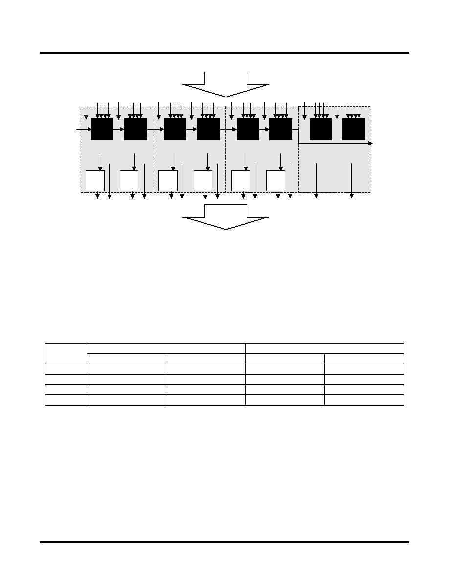
Figure 2-2. PFU Diagram
Slice
Slice 0 through Slice 2 contain two 4-input combinatorial Look-Up Tables (LUT4), which feed two registers. Slice 3
contains two LUT4s and no registers. For PFUs, Slice 0 and Slice 2 can also be configured as distributed memory,
a capability not available in PFF blocks. Table 2-1 shows the capability of the slices in both PFF and PFU blocks
along with the operation modes they enable. In addition, each PFU contains logic that allows the LUTs to be com-
bined to perform functions such as LUT5, LUT6, LUT7 and LUT8. There is control logic to perform set/reset func-
tions (programmable as synchronous/asynchronous), clock select, chip-select and wider RAM/ROM functions.
Figure 2-3 shows an overview of the internal logic of the slice. The registers in the slice can be configured as posi-
tive/negative edge triggered or level sensitive clocks.
Table 2-1. Resources and Modes Available per Slice
Slice 0 through Slice 2 have 14 input signals: 13 signals from routing and one from the carry-chain (from the adja-
cent slice or PFU). There are seven outputs: six to routing and one to carry-chain (to the adjacent PFU). Slice 3 has
13 input signals from routing and four signals to routing. Table 2-2 lists the signals associated with Slice 0 to Slice
2.
Slice
PFU BLock
PFF Block
Resources
Modes
Resources
Modes
Slice 0
2 LUT4s and 2 Registers Logic, Ripple, RAM, ROM 2 LUT4s and 2 Registers
Logic, Ripple, ROM
Slice 1
2 LUT4s and 2 Registers
Logic, Ripple, ROM
2 LUT4s and 2 Registers
Logic, Ripple, ROM
Slice 2
2 LUT4s and 2 Registers Logic, Ripple, RAM, ROM 2 LUT4s and 2 Registers
Logic, Ripple, ROM
Slice 3
2 LUT4s
Logic, ROM
2 LUT4s
Logic, ROM
Slice 0
LUT4 &
CARRY
LUT4 &
CARRY
D
Slice 1
LUT4 &
CARRY
LUT4 &
CARRY
Slice 2
LUT4 &
CARRY
LUT4 &
CARRY
From
Routing
To
Routing
Slice 3
LUT4
D
FF
相关PDF资料 |
PDF描述 |
|---|---|
| LFXP20E-3FN484C | |
| LFXP20E-5FN484C | |
| LFXP15C-4FN256C | |
| LFZ3508VXX | GENERAL PURPOSE INDUCTOR |
| LFZ2805HXX | GENERAL PURPOSE INDUCTOR |
相关代理商/技术参数 |
参数描述 |
|---|---|
| LFXP2-17E-7F484C8W | 功能描述:FPGA - 现场可编程门阵列 17KLUTs 358I/O Inst- on DSP 1.2V -7Spd RoHS:否 制造商:Altera Corporation 系列:Cyclone V E 栅极数量: 逻辑块数量:943 内嵌式块RAM - EBR:1956 kbit 输入/输出端数量:128 最大工作频率:800 MHz 工作电源电压:1.1 V 最大工作温度:+ 70 C 安装风格:SMD/SMT 封装 / 箱体:FBGA-256 |
| LFXP2-17E-7FN484C | 功能描述:FPGA - 现场可编程门阵列 17KLUTs 358 I/O Inst -on DSP 1.2V -6 Spd RoHS:否 制造商:Altera Corporation 系列:Cyclone V E 栅极数量: 逻辑块数量:943 内嵌式块RAM - EBR:1956 kbit 输入/输出端数量:128 最大工作频率:800 MHz 工作电源电压:1.1 V 最大工作温度:+ 70 C 安装风格:SMD/SMT 封装 / 箱体:FBGA-256 |
| LFXP2-17E-7FN484C8W | 功能描述:FPGA - 现场可编程门阵列 17KLUTs 358I/O Inst -on DSP 1.2V -7 Spd RoHS:否 制造商:Altera Corporation 系列:Cyclone V E 栅极数量: 逻辑块数量:943 内嵌式块RAM - EBR:1956 kbit 输入/输出端数量:128 最大工作频率:800 MHz 工作电源电压:1.1 V 最大工作温度:+ 70 C 安装风格:SMD/SMT 封装 / 箱体:FBGA-256 |
| LFXP2-17E-7FT256C | 功能描述:FPGA - 现场可编程门阵列 17KLUTs 201 I/O Inst -on DSP 1.2V -7 Spd RoHS:否 制造商:Altera Corporation 系列:Cyclone V E 栅极数量: 逻辑块数量:943 内嵌式块RAM - EBR:1956 kbit 输入/输出端数量:128 最大工作频率:800 MHz 工作电源电压:1.1 V 最大工作温度:+ 70 C 安装风格:SMD/SMT 封装 / 箱体:FBGA-256 |
| LFXP2-17E-7FT256C8W | 功能描述:FPGA - 现场可编程门阵列 17KLUTs 201 I/O Inst -on DSP 1.2V -7 Spd RoHS:否 制造商:Altera Corporation 系列:Cyclone V E 栅极数量: 逻辑块数量:943 内嵌式块RAM - EBR:1956 kbit 输入/输出端数量:128 最大工作频率:800 MHz 工作电源电压:1.1 V 最大工作温度:+ 70 C 安装风格:SMD/SMT 封装 / 箱体:FBGA-256 |
发布紧急采购,3分钟左右您将得到回复。