- 您现在的位置:买卖IC网 > PDF目录299403 > LFXP2-17E-7F484C (LATTICE SEMICONDUCTOR CORP) PDF资料下载
参数资料
| 型号: | LFXP2-17E-7F484C |
| 厂商: | LATTICE SEMICONDUCTOR CORP |
| 元件分类: | FPGA |
| 中文描述: | FPGA, 420 MHz, PBGA484 |
| 封装: | 23 X 23 MM, FPBGA-484 |
| 文件页数: | 7/92页 |
| 文件大小: | 1701K |
| 代理商: | LFXP2-17E-7F484C |
第1页第2页第3页第4页第5页第6页当前第7页第8页第9页第10页第11页第12页第13页第14页第15页第16页第17页第18页第19页第20页第21页第22页第23页第24页第25页第26页第27页第28页第29页第30页第31页第32页第33页第34页第35页第36页第37页第38页第39页第40页第41页第42页第43页第44页第45页第46页第47页第48页第49页第50页第51页第52页第53页第54页第55页第56页第57页第58页第59页第60页第61页第62页第63页第64页第65页第66页第67页第68页第69页第70页第71页第72页第73页第74页第75页第76页第77页第78页第79页第80页第81页第82页第83页第84页第85页第86页第87页第88页第89页第90页第91页第92页
2-12
Architecture
Lattice Semiconductor
LatticeXP2 Family Data Sheet
Primary Clock Routing
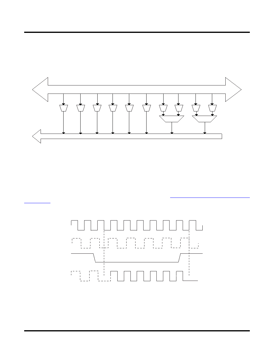
The clock routing structure in LatticeXP2 devices consists of a network of eight primary clock lines (CLK0 through
CLK7) per quadrant. The primary clocks of each quadrant are generated from muxes located in the center of the
device. All the clock sources are connected to these muxes. Figure 2-9 shows the clock routing for one quadrant.
Each quadrant mux is identical. If desired, any clock can be routed globally.
Figure 2-9. Per Quadrant Primary Clock Selection
Dynamic Clock Select (DCS)
The DCS is a smart multiplexer function available in the primary clock routing. It switches between two independent
input clock sources without any glitches or runt pulses. This is achieved irrespective of when the select signal is
toggled. There are two DCS blocks per quadrant; in total, eight DCS blocks per device. The inputs to the DCS block
come from the center muxes. The output of the DCS is connected to primary clocks CLK6 and CLK7 (see Figure 2-
9).
Figure 2-10 shows the timing waveforms of the default DCS operating mode. The DCS block can be programmed
to other modes. For more information on the DCS, please see TN1126, LatticeXP2 sysCLOCK PLL Design and
Figure 2-10. DCS Waveforms
Secondary Clock/Control Routing
Secondary clocks in the LatticeXP2 devices are region-based resources. The benefit of region-based resources is
the relatively low injection delay and skew within the region, as compared to primary clocks. EBR rows, DSP rows
and a special vertical routing channel bound the secondary clock regions. This special vertical routing channel
aligns with either the left edge of the center DSP block in the DSP row or the center of the DSP row. Figure 2-11
shows this special vertical routing channel and the eight secondary clock regions for the LatticeXP2-40.
CLK0
CLK1
CLK2
CLK3
CLK4
CLK5
CLK6
CLK7
30:1
29:1
30:1
8 Primary Clocks (CLK0 to CLK7) per Quadrant
DCS
Primary Clock Sources: PLLs + CLKDIVs + PIOs + Routing
CLK0
SEL
DCSOUT
CLK1
相关PDF资料 |
PDF描述 |
|---|---|
| LFXP20E-3FN484C | |
| LFXP20E-5FN484C | |
| LFXP15C-4FN256C | |
| LFZ3508VXX | GENERAL PURPOSE INDUCTOR |
| LFZ2805HXX | GENERAL PURPOSE INDUCTOR |
相关代理商/技术参数 |
参数描述 |
|---|---|
| LFXP2-17E-7F484C8W | 功能描述:FPGA - 现场可编程门阵列 17KLUTs 358I/O Inst- on DSP 1.2V -7Spd RoHS:否 制造商:Altera Corporation 系列:Cyclone V E 栅极数量: 逻辑块数量:943 内嵌式块RAM - EBR:1956 kbit 输入/输出端数量:128 最大工作频率:800 MHz 工作电源电压:1.1 V 最大工作温度:+ 70 C 安装风格:SMD/SMT 封装 / 箱体:FBGA-256 |
| LFXP2-17E-7FN484C | 功能描述:FPGA - 现场可编程门阵列 17KLUTs 358 I/O Inst -on DSP 1.2V -6 Spd RoHS:否 制造商:Altera Corporation 系列:Cyclone V E 栅极数量: 逻辑块数量:943 内嵌式块RAM - EBR:1956 kbit 输入/输出端数量:128 最大工作频率:800 MHz 工作电源电压:1.1 V 最大工作温度:+ 70 C 安装风格:SMD/SMT 封装 / 箱体:FBGA-256 |
| LFXP2-17E-7FN484C8W | 功能描述:FPGA - 现场可编程门阵列 17KLUTs 358I/O Inst -on DSP 1.2V -7 Spd RoHS:否 制造商:Altera Corporation 系列:Cyclone V E 栅极数量: 逻辑块数量:943 内嵌式块RAM - EBR:1956 kbit 输入/输出端数量:128 最大工作频率:800 MHz 工作电源电压:1.1 V 最大工作温度:+ 70 C 安装风格:SMD/SMT 封装 / 箱体:FBGA-256 |
| LFXP2-17E-7FT256C | 功能描述:FPGA - 现场可编程门阵列 17KLUTs 201 I/O Inst -on DSP 1.2V -7 Spd RoHS:否 制造商:Altera Corporation 系列:Cyclone V E 栅极数量: 逻辑块数量:943 内嵌式块RAM - EBR:1956 kbit 输入/输出端数量:128 最大工作频率:800 MHz 工作电源电压:1.1 V 最大工作温度:+ 70 C 安装风格:SMD/SMT 封装 / 箱体:FBGA-256 |
| LFXP2-17E-7FT256C8W | 功能描述:FPGA - 现场可编程门阵列 17KLUTs 201 I/O Inst -on DSP 1.2V -7 Spd RoHS:否 制造商:Altera Corporation 系列:Cyclone V E 栅极数量: 逻辑块数量:943 内嵌式块RAM - EBR:1956 kbit 输入/输出端数量:128 最大工作频率:800 MHz 工作电源电压:1.1 V 最大工作温度:+ 70 C 安装风格:SMD/SMT 封装 / 箱体:FBGA-256 |
发布紧急采购,3分钟左右您将得到回复。