- 您现在的位置:买卖IC网 > PDF目录1949 > MC68F375MZP33R2 (Freescale Semiconductor)IC MPU 32BIT 33MHZ 217-PBGA PDF资料下载
参数资料
| 型号: | MC68F375MZP33R2 |
| 厂商: | Freescale Semiconductor |
| 文件页数: | 202/616页 |
| 文件大小: | 0K |
| 描述: | IC MPU 32BIT 33MHZ 217-PBGA |
| 标准包装: | 500 |
| 系列: | M683xx |
| 处理器类型: | M683xx 32-位 |
| 速度: | 33MHz |
| 电压: | 5V |
| 安装类型: | 表面贴装 |
| 封装/外壳: | 217-BBGA |
| 供应商设备封装: | 217-PBGA(23x23) |
| 包装: | 带卷 (TR) |
第1页第2页第3页第4页第5页第6页第7页第8页第9页第10页第11页第12页第13页第14页第15页第16页第17页第18页第19页第20页第21页第22页第23页第24页第25页第26页第27页第28页第29页第30页第31页第32页第33页第34页第35页第36页第37页第38页第39页第40页第41页第42页第43页第44页第45页第46页第47页第48页第49页第50页第51页第52页第53页第54页第55页第56页第57页第58页第59页第60页第61页第62页第63页第64页第65页第66页第67页第68页第69页第70页第71页第72页第73页第74页第75页第76页第77页第78页第79页第80页第81页第82页第83页第84页第85页第86页第87页第88页第89页第90页第91页第92页第93页第94页第95页第96页第97页第98页第99页第100页第101页第102页第103页第104页第105页第106页第107页第108页第109页第110页第111页第112页第113页第114页第115页第116页第117页第118页第119页第120页第121页第122页第123页第124页第125页第126页第127页第128页第129页第130页第131页第132页第133页第134页第135页第136页第137页第138页第139页第140页第141页第142页第143页第144页第145页第146页第147页第148页第149页第150页第151页第152页第153页第154页第155页第156页第157页第158页第159页第160页第161页第162页第163页第164页第165页第166页第167页第168页第169页第170页第171页第172页第173页第174页第175页第176页第177页第178页第179页第180页第181页第182页第183页第184页第185页第186页第187页第188页第189页第190页第191页第192页第193页第194页第195页第196页第197页第198页第199页第200页第201页当前第202页第203页第204页第205页第206页第207页第208页第209页第210页第211页第212页第213页第214页第215页第216页第217页第218页第219页第220页第221页第222页第223页第224页第225页第226页第227页第228页第229页第230页第231页第232页第233页第234页第235页第236页第237页第238页第239页第240页第241页第242页第243页第244页第245页第246页第247页第248页第249页第250页第251页第252页第253页第254页第255页第256页第257页第258页第259页第260页第261页第262页第263页第264页第265页第266页第267页第268页第269页第270页第271页第272页第273页第274页第275页第276页第277页第278页第279页第280页第281页第282页第283页第284页第285页第286页第287页第288页第289页第290页第291页第292页第293页第294页第295页第296页第297页第298页第299页第300页第301页第302页第303页第304页第305页第306页第307页第308页第309页第310页第311页第312页第313页第314页第315页第316页第317页第318页第319页第320页第321页第322页第323页第324页第325页第326页第327页第328页第329页第330页第331页第332页第333页第334页第335页第336页第337页第338页第339页第340页第341页第342页第343页第344页第345页第346页第347页第348页第349页第350页第351页第352页第353页第354页第355页第356页第357页第358页第359页第360页第361页第362页第363页第364页第365页第366页第367页第368页第369页第370页第371页第372页第373页第374页第375页第376页第377页第378页第379页第380页第381页第382页第383页第384页第385页第386页第387页第388页第389页第390页第391页第392页第393页第394页第395页第396页第397页第398页第399页第400页第401页第402页第403页第404页第405页第406页第407页第408页第409页第410页第411页第412页第413页第414页第415页第416页第417页第418页第419页第420页第421页第422页第423页第424页第425页第426页第427页第428页第429页第430页第431页第432页第433页第434页第435页第436页第437页第438页第439页第440页第441页第442页第443页第444页第445页第446页第447页第448页第449页第450页第451页第452页第453页第454页第455页第456页第457页第458页第459页第460页第461页第462页第463页第464页第465页第466页第467页第468页第469页第470页第471页第472页第473页第474页第475页第476页第477页第478页第479页第480页第481页第482页第483页第484页第485页第486页第487页第488页第489页第490页第491页第492页第493页第494页第495页第496页第497页第498页第499页第500页第501页第502页第503页第504页第505页第506页第507页第508页第509页第510页第511页第512页第513页第514页第515页第516页第517页第518页第519页第520页第521页第522页第523页第524页第525页第526页第527页第528页第529页第530页第531页第532页第533页第534页第535页第536页第537页第538页第539页第540页第541页第542页第543页第544页第545页第546页第547页第548页第549页第550页第551页第552页第553页第554页第555页第556页第557页第558页第559页第560页第561页第562页第563页第564页第565页第566页第567页第568页第569页第570页第571页第572页第573页第574页第575页第576页第577页第578页第579页第580页第581页第582页第583页第584页第585页第586页第587页第588页第589页第590页第591页第592页第593页第594页第595页第596页第597页第598页第599页第600页第601页第602页第603页第604页第605页第606页第607页第608页第609页第610页第611页第612页第613页第614页第615页第616页
MC68F375
QUEUED SERIAL MULTI-CHANNEL MODULE
MOTOROLA
REFERENCE MANUAL
Rev. 25 June 03
6-46
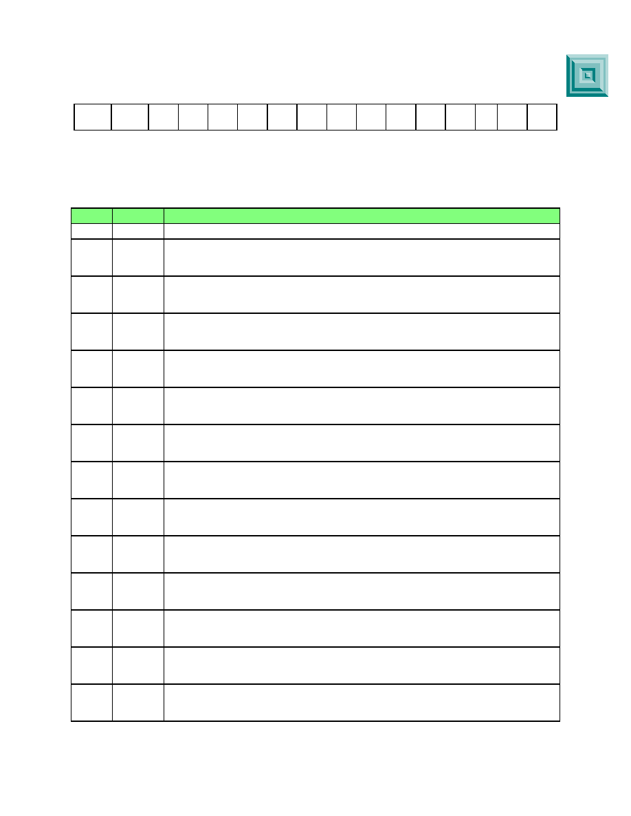
SCCxR1 — SCI Control Register 1
0xYF FC0A, 0xYF FC22
MSB
15
14
13
12
11
10
9
8
7
6
5
4
3
2
1
LSB
0
LOOPS
WOM
S
ILT
PT
PE
M
WAKE
TIE
TCIE
RIE
ILIE
TE
RE
RWU
SBK
RESET:
0
Table 6-24 SCCxR1 Bit Settings
Bit(s)
Name
Description
15
—
Reserved
14
LOOPS
Loop mode
0 = Normal SCI operation, no looping, feedback path disabled.
1 = SCI test operation, looping, feedback path enabled.
13
WOMS
Wired-OR mode for SCI Pins
0 = If configured as an output, TXD is a normal CMOS output.
1 = If configured as an output, TXD is an open drain output.
12
ILT
Idle-line detect type. Refer to 6.8.7.7 Idle-Line Detection.
0 = Short idle-line detect (start count on first one).
1 = Long idle-line detect (start count on first one after stop bit(s)).
11
PT
Parity type. Refer to 6.8.7.4 Parity Checking.
0 = Even parity.
1 = Odd parity.
10
PE
Parity enable. Refer to 6.8.7.4 Parity Checking.
0 = SCI parity disabled.
1 = SCI parity enabled.
9M
Mode select. Refer to 6.8.7.2 Serial Formats.
0 = 10-bit SCI frame.
1 = 11-bit SCI frame.
8
WAKE
Wakeup by address mark. Refer to 6.8.7.8 Receiver Wake-Up.
0 = SCI receiver awakened by idle-line detection.
1 = SCI receiver awakened by address mark (last bit set).
7TIE
Transmit interrupt enable
0 = SCI TDRE interrupts disabled.
1 = SCI TDRE interrupts enabled.
6TCIE
Transmit complete interrupt enable
0 = SCI TC interrupts disabled.
1 = SCI TC interrupts enabled.
5RIE
Receiver interrupt enable
0 = SCI RDRF and OR interrupts disabled.
1 = SCI RDRF and OR interrupts enabled.
4ILIE
Idle-line interrupt enable
0 = SCI IDLE interrupts disabled.
1 = SCI IDLE interrupts enabled.
3TE
Transmitter enable
0 = SCI transmitter disabled (TXD pin can be used as general-purpose output)
1 = SCI transmitter enabled (TXD pin dedicated to SCI transmitter).
2RE
Receiver Enable
0 = SCI receiver disabled (RXD pin can be used as general-purpose input).
1 = SCI receiver enabled (RXD pin is dedicated to SCI receiver).
F
re
e
sc
a
le
S
e
m
ic
o
n
d
u
c
to
r,
I
Freescale Semiconductor, Inc.
For More Information On This Product,
Go to: www.freescale.com
n
c
..
.
相关PDF资料 |
PDF描述 |
|---|---|
| MC68HC001CEI8 | IC MPU 32BIT 8MHZ 68-PLCC |
| MC68HC11K1VFNE4 | MCU 8-BIT 768 RAM 4MHZ 84-PLCC |
| MC68HC16Z1CPV25 | IC MPU 1K RAM 25MHZ 144-LQFP |
| MC68HC16Z1VEH16 | IC MCU 16BIT 1K FLASH 132-PQFP |
| MC68HC705B16NCFN | IC MCU 2.1MHZ 15K OTP 52-PLCC |
相关代理商/技术参数 |
参数描述 |
|---|---|
| MC68H(R)C08JK1 | 制造商:MOTOROLA 制造商全称:Motorola, Inc 功能描述:HCMOS Microcontroller Unit |
| MC68H(R)C08JK3 | 制造商:MOTOROLA 制造商全称:Motorola, Inc 功能描述:HCMOS Microcontroller Unit |
| MC68H(R)C08JL3 | 制造商:MOTOROLA 制造商全称:Motorola, Inc 功能描述:HCMOS Microcontroller Unit |
| MC68H705C8A | 制造商:Motorola Inc 功能描述: |
| MC68HC | 制造商:FREESCALE 制造商全称:Freescale Semiconductor, Inc 功能描述:Power Saving STOP and WAIT Modes |
发布紧急采购,3分钟左右您将得到回复。