- 您现在的位置:买卖IC网 > PDF目录385639 > MT46V4M32 (Micron Technology, Inc.) DOUBLE DATA RATE DDR SDRAM PDF资料下载
参数资料
| 型号: | MT46V4M32 |
| 厂商: | Micron Technology, Inc. |
| 英文描述: | DOUBLE DATA RATE DDR SDRAM |
| 中文描述: | 双倍数据速率的DDR SDRAM内存 |
| 文件页数: | 9/66页 |
| 文件大小: | 1921K |
| 代理商: | MT46V4M32 |
第1页第2页第3页第4页第5页第6页第7页第8页当前第9页第10页第11页第12页第13页第14页第15页第16页第17页第18页第19页第20页第21页第22页第23页第24页第25页第26页第27页第28页第29页第30页第31页第32页第33页第34页第35页第36页第37页第38页第39页第40页第41页第42页第43页第44页第45页第46页第47页第48页第49页第50页第51页第52页第53页第54页第55页第56页第57页第58页第59页第60页第61页第62页第63页第64页第65页第66页
9
128Mb: x32 DDR SDRAM
4M32DDR_B.p65 – Rev. B, Pub. 7/02
Micron Technology, Inc., reserves the right to change products or specifications without notice.
2002, Micron Technology, Inc.
128Mb: x32
DDR SDRAM
ADVANCE
lected by A1-A
i
when the burst length is set to two, by
A2-A
i
when the burst length is set to four and by A3-A
i
when the burst length is set to eight (where A
i
is the
most significant column address bit for a given con-
figuration). The remaining (least significant) address
bit(s) is (are) used to select the starting location within
the block. The programmed burst length applies to
both READ and WRITE bursts.
Burst Type
Accesses within a given burst may be programmed
to be either sequential or interleaved; this is referred to
as the burst type and is selected via bit M3.
The ordering of accesses within a burst is deter-
mined by the burst length, the burst type and the start-
ing column address, as shown in Table 1.
Figure 2
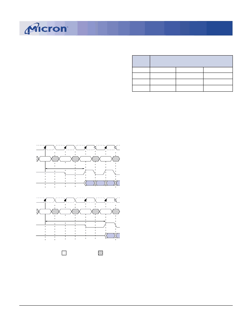
CAS Latency
Read Latency
The READ latency is the delay, in clock cycles, be-
tween the registration of a READ command and the
availability of the first bit of output data. The latency
can be set to 2, 3, 4 or 5 clocks, as shown in Figure 2.
If a READ command is registered at clock edge
n
, and
the latency is
m
clocks, the data will be available nominally
coincident with clock edge
n + m
. Table 2 indicates the
operating frequencies at which each CAS latency setting
can be used.
Reserved states should not be used as unknown
operation or incompatibility with future versions may
result.
Operating Mode
The normal operating mode is selected by issuing a
MODE REGISTER SET command with bits A7-A11 each
set to zero, and bits A0-A6 set to the desired values. A
DLL reset is initiated by issuing a MODE REGISTER
CK
CK#
COMMAND
DQ
DQS
CL = 2
READ
NOP
NOP
NOP
READ
NOP
NOP
NOP
Burst Length = 4 in the cases shown
Shown with nominal tAC and nominal tDSDQ
CK
CK#
COMMAND
DQ
DQS
CL = 3
T0
T1
T2
T2n
T3
T3n
T0
T1
T2
T3
T3n
DON’T CARE
TRANSITIONING DATA
Table 2
CAS Latency
ALLOWABLE OPERATING
FREQUENCY (MHz)
CL = 5
CL = 4
≤
300
≤
250
≤
250
SPEED
-33
-4
-5
CL = 3
≤
200
≤
200
相关PDF资料 |
PDF描述 |
|---|---|
| MT46V4M32LG | I.MX31 LITE KIT |
| MT46V64M4 | 16 Meg x 4 x 4 banks DDR SDRAM(16M x 4 x 4组,双数据速率同步动态RAM) |
| MT46V64M8 | 16 Meg x 8 x 4 banks DDR SDRAM(16M x 8 x 4组,双数据速率同步动态RAM) |
| MT48LC16M8A1TG | SYNCHRONOUS DRAM |
| MT48LC32M4A1 | ECONOLINE: RSZ/P - 1kVDC |
相关代理商/技术参数 |
参数描述 |
|---|---|
| MT46V4M32LG | 制造商:MICRON 制造商全称:Micron Technology 功能描述:DOUBLE DATA RATE DDR SDRAM |
| MT46V64M16 | 制造商:MICRON 制造商全称:Micron Technology 功能描述:DOUBLE DATA RATE (DDR) SDRAM |
发布紧急采购,3分钟左右您将得到回复。