- 您现在的位置:买卖IC网 > PDF目录230133 > NAND256W3A0AN6F (NUMONYX) 32M X 8 FLASH 3V PROM, 35 ns, PDSO48 PDF资料下载
参数资料
| 型号: | NAND256W3A0AN6F |
| 厂商: | NUMONYX |
| 元件分类: | PROM |
| 英文描述: | 32M X 8 FLASH 3V PROM, 35 ns, PDSO48 |
| 封装: | 12 X 20 MM, ROHS COMPLIANT, PLASTIC, TSOP-48 |
| 文件页数: | 21/58页 |
| 文件大小: | 1406K |
| 代理商: | NAND256W3A0AN6F |
第1页第2页第3页第4页第5页第6页第7页第8页第9页第10页第11页第12页第13页第14页第15页第16页第17页第18页第19页第20页当前第21页第22页第23页第24页第25页第26页第27页第28页第29页第30页第31页第32页第33页第34页第35页第36页第37页第38页第39页第40页第41页第42页第43页第44页第45页第46页第47页第48页第49页第50页第51页第52页第53页第54页第55页第56页第57页第58页
Device operations
NAND128-A, NAND256-A
6.5
Block erase
Erase operations are done one block at a time. An erase operation sets all of the bits in the
addressed block to ‘1’. All previous data in the block is lost.
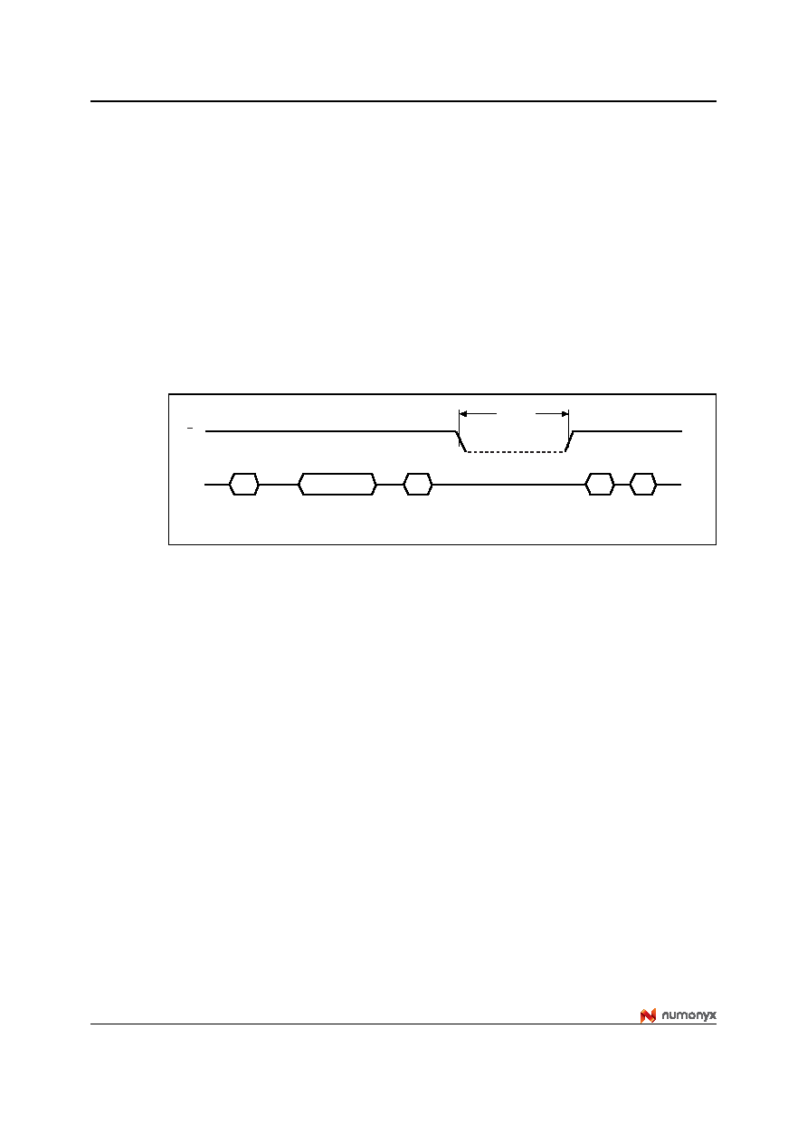
An erase operation consists of the following three steps (refer to Figure 16: Block erase
1.
One bus cycle is required to set up the Block Erase command.
2.
Only two bus cycles are required to input the block address. The first cycle (A0 to A7) is
not required as only addresses A14 to A26 (highest address depends on device
density) are valid, A9 to A13 are ignored. In the last address cycle I/O2 to I/O7 must be
set to VIL.
3.
One bus cycle is required to issue the confirm command to start the P/E/R controller.
Once the erase operation has completed the status register can be checked for errors.
Figure 16.
Block erase operation
6.6
Reset
The Reset command resets the command interface and status register. If the Reset
command is issued during any operation, the operation is aborted. If it was a program or
erase operation that was aborted, the contents of the memory locations being modified are
no longer valid as the data is partially programmed or erased.
If the device has already been reset then the new Reset command is not accepted.
The Ready/Busy signal goes Low for tBLBH4 after the Reset command is issued. The value
of tBLBH4 depends on the operation that the device was performing when the command was
issued (refer to Table 20: AC characteristics for operations for the values.)
6.7
Read status register
The device contains a status register which provides information on the current or previous
program or erase operation. the various bits in the status register convey information and
errors on the operation.
the status register is read by issuing the read status register command. the status register
information is present on the output data bus (I/O0-I/O7) on the falling edge of chip enable
or read enable, whichever occurs last. when several memories are connected in a system,
the use of chip enable and read enable signals allows the system to poll each device
separately, even when the ready/busy pins are common-wired. it is not necessary to toggle
the chip enable or read enable signals to update the contents of the status register.
I/O
RB
Block Address
Inputs
SR0
ai07593
D0h
70h
60h
Block Erase
Setup Code
Confirm
Code
Read Status Register
Busy
tBLBH3
(Erase Busy time)
相关PDF资料 |
PDF描述 |
|---|---|
| NAND512W3A0AN1T | 64M X 8 FLASH 3V PROM, 35 ns, PDSO48 |
| NAND512W3A0AN6T | 64M X 8 FLASH 3V PROM, 35 ns, PDSO48 |
| NAND512W3A0BZB1E | 64M X 8 FLASH 3V PROM, 35 ns, PBGA55 |
| NAND512W3A2AZB1E | 64M X 8 FLASH 3V PROM, 35 ns, PBGA55 |
| NAND01GW3A3AZA1T | 128M X 8 FLASH 3V PROM, 12000 ns, PBGA63 |
相关代理商/技术参数 |
参数描述 |
|---|---|
| NAND256W3A0AZA6E | 制造商:Micron Technology Inc 功能描述:FLASH PARALLEL 2.7V TO 3.6V 256MBIT 32MX8 12US 55VFBGA - Trays |
| NAND256W3A0AZA6F | 制造商:Micron Technology Inc 功能描述:FLASH PARALLEL 2.7V TO 3.6V 256MBIT 32MX8 12US 55VFBGA - Tape and Reel |
| NAND256W3A0BE06 | 功能描述:闪存 NAND & S.MEDIA FLASH RoHS:否 制造商:ON Semiconductor 数据总线宽度:1 bit 存储类型:Flash 存储容量:2 MB 结构:256 K x 8 定时类型: 接口类型:SPI 访问时间: 电源电压-最大:3.6 V 电源电压-最小:2.3 V 最大工作电流:15 mA 工作温度:- 40 C to + 85 C 安装风格:SMD/SMT 封装 / 箱体: 封装:Reel |
| NAND256W3A0BN6E | 制造商:Micron Technology Inc 功能描述:NAND - Trays |
| NAND256W3A0BN6F | 制造商:Micron Technology Inc 功能描述:NAND - Tape and Reel |
发布紧急采购,3分钟左右您将得到回复。