- 您现在的位置:买卖IC网 > PDF目录189449 > OR4E063BM680-DB (LATTICE SEMICONDUCTOR CORP) FPGA, 2024 CLBS, 515000 GATES, PBGA680 PDF资料下载
参数资料
| 型号: | OR4E063BM680-DB |
| 厂商: | LATTICE SEMICONDUCTOR CORP |
| 元件分类: | FPGA |
| 英文描述: | FPGA, 2024 CLBS, 515000 GATES, PBGA680 |
| 封装: | PLASTIC, FBGA-680 |
| 文件页数: | 100/151页 |
| 文件大小: | 2680K |
| 代理商: | OR4E063BM680-DB |
第1页第2页第3页第4页第5页第6页第7页第8页第9页第10页第11页第12页第13页第14页第15页第16页第17页第18页第19页第20页第21页第22页第23页第24页第25页第26页第27页第28页第29页第30页第31页第32页第33页第34页第35页第36页第37页第38页第39页第40页第41页第42页第43页第44页第45页第46页第47页第48页第49页第50页第51页第52页第53页第54页第55页第56页第57页第58页第59页第60页第61页第62页第63页第64页第65页第66页第67页第68页第69页第70页第71页第72页第73页第74页第75页第76页第77页第78页第79页第80页第81页第82页第83页第84页第85页第86页第87页第88页第89页第90页第91页第92页第93页第94页第95页第96页第97页第98页第99页当前第100页第101页第102页第103页第104页第105页第106页第107页第108页第109页第110页第111页第112页第113页第114页第115页第116页第117页第118页第119页第120页第121页第122页第123页第124页第125页第126页第127页第128页第129页第130页第131页第132页第133页第134页第135页第136页第137页第138页第139页第140页第141页第142页第143页第144页第145页第146页第147页第148页第149页第150页第151页
52
Lattice Semiconductor
Data Sheet
September, 2002
ORCA Series 4 FPGAs
Microprocessor Interface (continued)
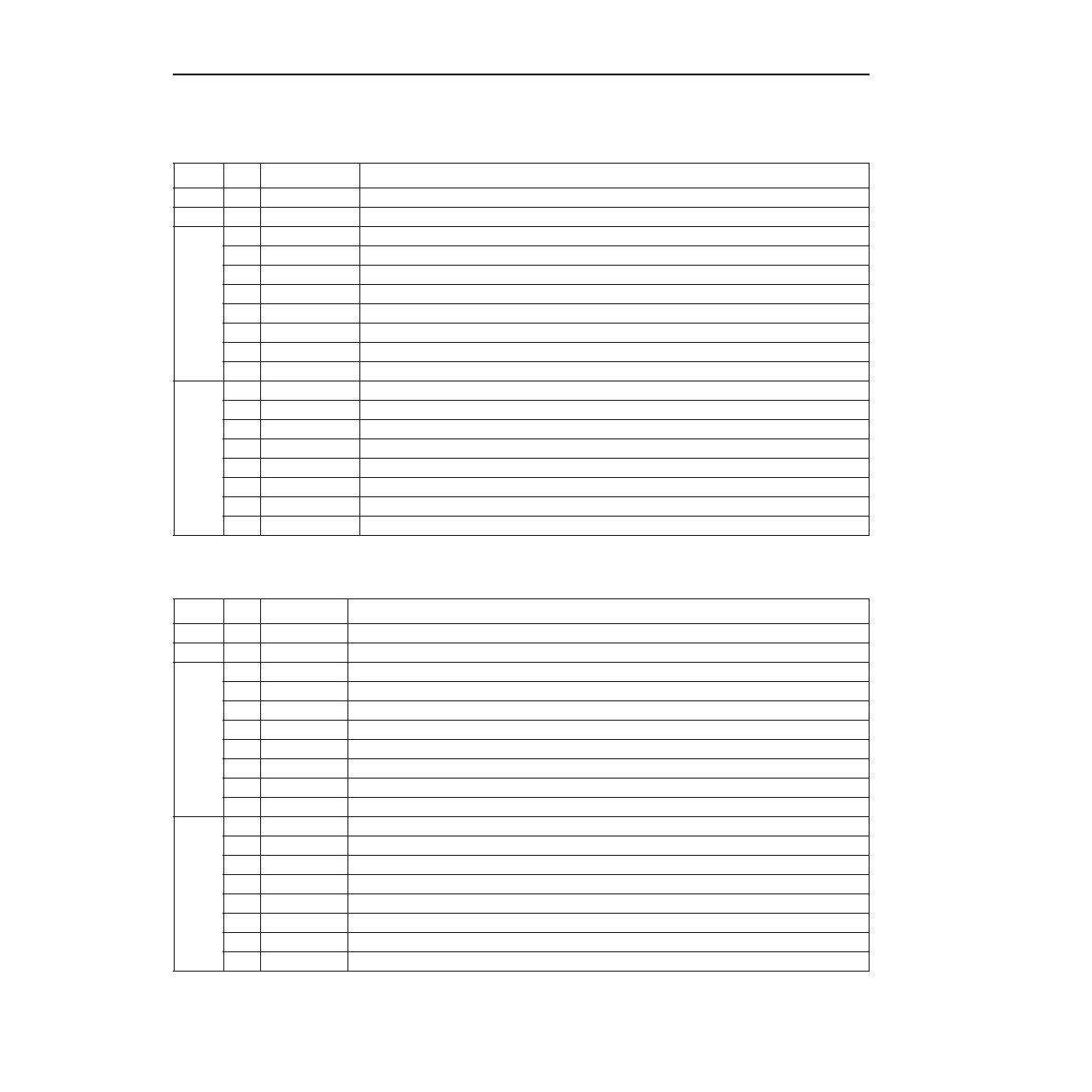
Table 25. Status Register Space Assignments
Notes: RO = Read Only. For internal system bus, bit 7 is most signicant bit, for MPI bit 0 is most signicant bit.
Table 26. Command Register Space Assignments
Note: R/W = Read/Write. For internal system bus; bit 7 is most signicant bit, for MPI bit 0 is most signicant bit.
Byte
bit
Read/Write
Description
0F
7:0
—
Reserved
0E
7:0
—
Reserved
OD
7
RO
Conguration Write Data Acknowledge
6RO
Readback Data Ready
5RO
Unassigned (Zero)
4RO
Unassigned (Zero)
3RO
FPSC_BIT_ERR
2RO
RAM_BIT_ERR
1RO
Conguration Write Data Size (1, 2, or 4 bytes)
0RO
Use with above for HSIZE[1:0] (byte, half-word, word)
0C
7
RO
Readback Addresses Out of Range
6RO
Error Response Received by CFG From System Bus
5RO
Error Responses Received by CFG From System Bus
4RO
CFG_DATA_LOST
3RO
DONE
2RO
INIT_N
1RO
ERR_FLAG 1
0RO
ERR_FLAG 0
Byte
bit
Read/Write
Description
0B
7:0
—
Reserved
0A
7:0
—
Reserved
09
7
R/W
SYS_GSR (GSR Input)
6
R/W
SYS_RD_CFG (similar to FPGA pin RD_CFGN, but active high)
5
R/W
PRGM from MPI > (similar to FPGA pin, but active high)
4
R/W
PRGM from USER > (similar to FPGA pin, but active high)
3
R/W
PRGM from FPSC > (similar to FPGA pin, but active high)
2
R/W
LOCK from MPI
1
R/W
LOCK from USER
0
R/W
LOCK from FPSC
08
7
R/W
Bus Reset from MPI (resets system bus and registers)
6
R/W
Bus Reset from USER (resets system bus and registers)
5
R/W
Bus Reset from FPSC (resets system bus and registers)
4
R/W
SYS_DAISY
3
R/W
REPEAT_RDBK (don't increment readback address)
2
R/W
MPI_USR_ENABLE
1
R/W
Readback Data Size (1, 2, or 4 bytes)
0
R/W
Use with above for HSIZE[1:0]
相关PDF资料 |
PDF描述 |
|---|---|
| ORT4622-8BC432I | FPGA, PBGA432 |
| ORT4622-8BM680I | FPGA, PBGA680 |
| ORT4622-8BC432I | FPGA, PBGA432 |
| ORT4622-8BM680I | FPGA, PBGA680 |
| ORT4622-8BC432I | FPGA, PBGA432 |
相关代理商/技术参数 |
参数描述 |
|---|---|
| OR4E10 | 制造商:AGERE 制造商全称:AGERE 功能描述:Field-Programmable Gate Arrays |
| OR4E14 | 制造商:未知厂家 制造商全称:未知厂家 功能描述:Field-Programmable Gate Arrays |
| OR4E2 | 制造商:AGERE 制造商全称:AGERE 功能描述:Field-Programmable Gate Arrays |
| OR4E2-1BA256 | 制造商:未知厂家 制造商全称:未知厂家 功能描述:FPGA |
| OR4E2-1BA352 | 制造商:未知厂家 制造商全称:未知厂家 功能描述:FPGA |
发布紧急采购,3分钟左右您将得到回复。