- 您现在的位置:买卖IC网 > PDF目录189449 > OR4E063BM680-DB (LATTICE SEMICONDUCTOR CORP) FPGA, 2024 CLBS, 515000 GATES, PBGA680 PDF资料下载
参数资料
| 型号: | OR4E063BM680-DB |
| 厂商: | LATTICE SEMICONDUCTOR CORP |
| 元件分类: | FPGA |
| 英文描述: | FPGA, 2024 CLBS, 515000 GATES, PBGA680 |
| 封装: | PLASTIC, FBGA-680 |
| 文件页数: | 137/151页 |
| 文件大小: | 2680K |
| 代理商: | OR4E063BM680-DB |
第1页第2页第3页第4页第5页第6页第7页第8页第9页第10页第11页第12页第13页第14页第15页第16页第17页第18页第19页第20页第21页第22页第23页第24页第25页第26页第27页第28页第29页第30页第31页第32页第33页第34页第35页第36页第37页第38页第39页第40页第41页第42页第43页第44页第45页第46页第47页第48页第49页第50页第51页第52页第53页第54页第55页第56页第57页第58页第59页第60页第61页第62页第63页第64页第65页第66页第67页第68页第69页第70页第71页第72页第73页第74页第75页第76页第77页第78页第79页第80页第81页第82页第83页第84页第85页第86页第87页第88页第89页第90页第91页第92页第93页第94页第95页第96页第97页第98页第99页第100页第101页第102页第103页第104页第105页第106页第107页第108页第109页第110页第111页第112页第113页第114页第115页第116页第117页第118页第119页第120页第121页第122页第123页第124页第125页第126页第127页第128页第129页第130页第131页第132页第133页第134页第135页第136页当前第137页第138页第139页第140页第141页第142页第143页第144页第145页第146页第147页第148页第149页第150页第151页
86
Lattice Semiconductor
Data Sheet
September, 2002
ORCA Series 4 FPGAs
TimingCharacteristics(continued)
Table49.PrimaryClockSkewtoanyPFUorPIORegister
OR4Exxx industrial: VDD15 = 1.425 V to 1.575 V, VDD33 = 3.0 V to 3.6 V, –40 °C
< TJ < +125 °C.
Table50.SecondaryClocktoOutputDelaywithouton-chipPLLs(Pin-to-Pin)
OR4Exxx industrial: VDD15 = 1.425 V to 1.575 V, VDD33 = 3.0 V to 3.6 V, VDDIO = 3.0 V to 3.6 V, –40 °C
< TJ
< +85 °C.; CL = 30 pF.
Notes:
1. Timingiswithouttheuseofthephase-lockedloops(PLLs).
2. Thisclockdelayisforafullyroutedclocktreethatusesthesecondaryclocknetwork.ItincludestheLVTTL(3.3V)inputclockbuffer,the
clockroutingtothePIOCLKinput,theclock→QoftheFF,andthedelaythroughtheLVTTL(3.3V)dataoutputbuffer.AnSCLKinputclock
canbeatanyinputpin.
3. FortimingimprovementsusingotherI/Obuffertypesfortheinputclockbufferoroutputdatabuffer,seeTable45andTable47.
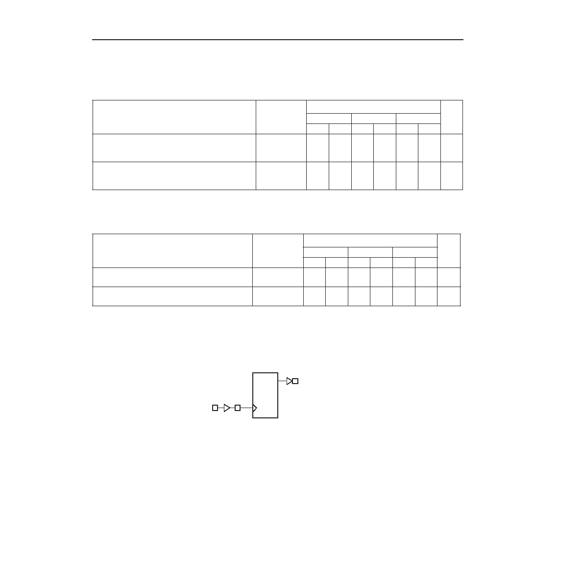
5-4846(F).a
Figure48.SecondaryCLKtoOutputDelay
Description
Device
Speed
Unit
-1
-2
-3
Min
Max
Min
Max
Min
Max
PrimaryClockSkewInformation(posedgeto
posedgeornegedgetonegedge)
OR4E02
OR4E04
OR4E06
—
85
110
120
—
75
95
105
—
70
90
100
ps
PrimaryClockSkewInformation(posedgeto
posedge,negedgetonegedge,posedgeto
negedgeornegedgetoposedge)
OR4E02
OR4E04
OR4E06
—
265
285
300
—
190
210
220
—
180
200
210
ps
Description
Device
Speed
Unit
-1
-2
-3
Min
Max
Min
Max
Min
Max
SCLK→ OUTPUTPin(LVTTL-12mAFast,
Outputwithin6PICsofSCLKinput)
All
—
7.22
—
6.70
—
6.06
ns
AdditionalDelaypereachextra6PICsper
clockroutedirection.
All
—
0.36
—
0.38
—
0.34
ns
OUTPUT(30pFLOAD)
Q
D
SCLK
PIOFF
相关PDF资料 |
PDF描述 |
|---|---|
| ORT4622-8BC432I | FPGA, PBGA432 |
| ORT4622-8BM680I | FPGA, PBGA680 |
| ORT4622-8BC432I | FPGA, PBGA432 |
| ORT4622-8BM680I | FPGA, PBGA680 |
| ORT4622-8BC432I | FPGA, PBGA432 |
相关代理商/技术参数 |
参数描述 |
|---|---|
| OR4E10 | 制造商:AGERE 制造商全称:AGERE 功能描述:Field-Programmable Gate Arrays |
| OR4E14 | 制造商:未知厂家 制造商全称:未知厂家 功能描述:Field-Programmable Gate Arrays |
| OR4E2 | 制造商:AGERE 制造商全称:AGERE 功能描述:Field-Programmable Gate Arrays |
| OR4E2-1BA256 | 制造商:未知厂家 制造商全称:未知厂家 功能描述:FPGA |
| OR4E2-1BA352 | 制造商:未知厂家 制造商全称:未知厂家 功能描述:FPGA |
发布紧急采购,3分钟左右您将得到回复。