- 您现在的位置:买卖IC网 > PDF目录69042 > PC34708VM (FREESCALE SEMICONDUCTOR INC) 1-CHANNEL POWER SUPPLY MANAGEMENT CKT, PBGA206 PDF资料下载
参数资料
| 型号: | PC34708VM |
| 厂商: | FREESCALE SEMICONDUCTOR INC |
| 元件分类: | 电源管理 |
| 英文描述: | 1-CHANNEL POWER SUPPLY MANAGEMENT CKT, PBGA206 |
| 封装: | 13 X 13 MM, 0.80 MM PITCH, LEAD FREE, MO-275HHAC-1, MAPBGA-206 |
| 文件页数: | 6/200页 |
| 文件大小: | 5160K |
| 代理商: | PC34708VM |
第1页第2页第3页第4页第5页当前第6页第7页第8页第9页第10页第11页第12页第13页第14页第15页第16页第17页第18页第19页第20页第21页第22页第23页第24页第25页第26页第27页第28页第29页第30页第31页第32页第33页第34页第35页第36页第37页第38页第39页第40页第41页第42页第43页第44页第45页第46页第47页第48页第49页第50页第51页第52页第53页第54页第55页第56页第57页第58页第59页第60页第61页第62页第63页第64页第65页第66页第67页第68页第69页第70页第71页第72页第73页第74页第75页第76页第77页第78页第79页第80页第81页第82页第83页第84页第85页第86页第87页第88页第89页第90页第91页第92页第93页第94页第95页第96页第97页第98页第99页第100页第101页第102页第103页第104页第105页第106页第107页第108页第109页第110页第111页第112页第113页第114页第115页第116页第117页第118页第119页第120页第121页第122页第123页第124页第125页第126页第127页第128页第129页第130页第131页第132页第133页第134页第135页第136页第137页第138页第139页第140页第141页第142页第143页第144页第145页第146页第147页第148页第149页第150页第151页第152页第153页第154页第155页第156页第157页第158页第159页第160页第161页第162页第163页第164页第165页第166页第167页第168页第169页第170页第171页第172页第173页第174页第175页第176页第177页第178页第179页第180页第181页第182页第183页第184页第185页第186页第187页第188页第189页第190页第191页第192页第193页第194页第195页第196页第197页第198页第199页第200页
Analog Integrated Circuit Device Data
Freescale Semiconductor
103
PC34708
Functional Block Requirements and Behaviors
32.768 kHz Crystal Oscillator RTC Block Description and Application Information
7.9.2.2
Real Time Clock
A Real Time Clock (RTC) is provided with time and day counters as well as an alarm function. The RTC utilizes the 32.768 kHz
crystal oscillator for the time base and is powered by the coin cell backup supply when BP has dropped below operational range.
In configurations where the SRTC is used, the RTC can be disabled to conserve current drain by setting the RTCDIS bit to a 1
(defaults on at power up).
Time and Day Counters
The 32.768 kHz clock is divided down to a 1.0 Hz time tick which drives a 17 bit Time Of Day (TOD) counter. The TOD counter
counts the seconds during a 24 hour period from 0 to 86,399 and will then roll over to 0. When the roll over occurs, it increments
the 15 bit DAY counter. The DAY counter can count up to 32767 days. The 1.0 Hz time tick can be used to generate a 1HZI
interrupt if unmasked.
Time Of Day Alarm
A Time Of Day Alarm (TODA) function can be used to turn on the application and alert the processor. If the application is already
on, the processor will be interrupted. The TODA and DAYA registers are used to set the alarm time. When the TOD counter is
equal to the value in TODA and the DAY counter is equal to the value in DAYA, the TODAI interrupt will be generated.
Timer Reset
As long as the supply at BP is valid, the real time clock will be supplied from VCOREDIG. If BP is not valid, the real time clock
can be backed up from a coin cell via the LICELL pin. When the VSRTC voltage drops to the range of 0.9 - 0.8 V, the RTCPORB
reset signal is generated and the contents of the RTC will be reset. Additional registers backed up by coin cell will also reset with
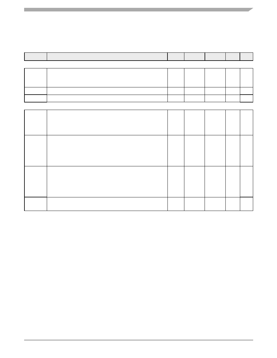
Table 106. VSRTC Electrical Specifications
Characteristics noted under conditions BP = 3.6 V, VBUS = 5.0 V, -40°C ≤ TA ≤ 85°C, unless otherwise noted. Typical values at
BP = 3.6 V and TA = 25°C under nominal conditions, unless otherwise noted.
Symbol
Characteristic
Min
Typ
Max
Unit
Notes
GENERAL
VSRTCIN
Operating Input Voltage Range VINMIN to VINMAX
Valid Coin Cell range
Valid BP
1.8
-
3.6
4.5
V
ISRTC
Operating Current Load Range ILMIN to ILMAX
0
-
50
μA
COSRTC
Bypass Capacitor Value
-
0.1
-
μF
VSRTC - ACTIVE MODE - DC
VSRTC
Output Voltage VOUT
VINMIN < VIN < VINMAX
ILMIN < IL < ILMAX
Off and coincell mode
1.15
1.20
1.28
V
VSRTC
Output Voltage VOUT
VINMIN < VIN < VINMAX
ILMIN < IL < ILMAX
PUMS[4:0] = (0110, 0111, 1000, 1001)
On mode (On, Standby, Standby LPM)
1.15
1.2
1.25
V
VSRTC
Output Voltage VOUT
VINMIN < VIN < VINMAX
ILMIN < IL < ILMAX
PUMS[4:0] = (0110, 0111, 1000, 1001)
On mode (On, Standby, Standby LPM)
1.25
1.3
1.35
V
ISRTCQ
Active Mode Quiescent Current
VINMIN < VIN < VINMAX IL = 0
-
0.8
-
μA
相关PDF资料 |
PDF描述 |
|---|---|
| PC34708VK | 1-CHANNEL POWER SUPPLY MANAGEMENT CKT, PBGA206 |
| PCF1252-6T | 1-CHANNEL POWER SUPPLY SUPPORT CKT, PDSO8 |
| PCF1252-8T-T | 1-CHANNEL POWER SUPPLY SUPPORT CKT, PDSO8 |
| PCF1252-4T-T | 1-CHANNEL POWER SUPPLY SUPPORT CKT, PDSO8 |
| PCF1252-4T | 1-CHANNEL POWER SUPPLY SUPPORT CKT, PDSO8 |
相关代理商/技术参数 |
参数描述 |
|---|---|
| PC34709VK | 制造商:Freescale Semiconductor 功能描述:PMIC 5SW,6 LDO,BST - Bulk |
| PC34709VKR2 | 制造商:Freescale Semiconductor 功能描述:PMIC 5SW,6 LDO,BST - Tape and Reel |
| PC34710EW | 制造商:MOTOROLA 制造商全称:Motorola, Inc 功能描述:Adjustable Dual Output Switching Power Supply |
| PC34710EWR2 | 制造商:MOTOROLA 制造商全称:Motorola, Inc 功能描述:Adjustable Dual Output Switching Power Supply |
| PC3-48-12 | 功能描述:DC/DC转换器 3W 12V 0.25A RoHS:否 制造商:Murata 产品: 输出功率: 输入电压范围:3.6 V to 5.5 V 输入电压(标称): 输出端数量:1 输出电压(通道 1):3.3 V 输出电流(通道 1):600 mA 输出电压(通道 2): 输出电流(通道 2): 安装风格:SMD/SMT 封装 / 箱体尺寸: |
发布紧急采购,3分钟左右您将得到回复。