- 您现在的位置:买卖IC网 > PDF目录378049 > PEF2256H (INFINEON TECHNOLOGIES AG) Ultraframer DS3/E3/DS2/E2/DS1/E1/DS0 PDF资料下载
参数资料
| 型号: | PEF2256H |
| 厂商: | INFINEON TECHNOLOGIES AG |
| 元件分类: | 通信及网络 |
| 英文描述: | Ultraframer DS3/E3/DS2/E2/DS1/E1/DS0 |
| 中文描述: | Ultraframer DS3/E3/DS2/E2/DS1/E1/DS0 |
| 文件页数: | 105/518页 |
| 文件大小: | 6420K |
| 代理商: | PEF2256H |
第1页第2页第3页第4页第5页第6页第7页第8页第9页第10页第11页第12页第13页第14页第15页第16页第17页第18页第19页第20页第21页第22页第23页第24页第25页第26页第27页第28页第29页第30页第31页第32页第33页第34页第35页第36页第37页第38页第39页第40页第41页第42页第43页第44页第45页第46页第47页第48页第49页第50页第51页第52页第53页第54页第55页第56页第57页第58页第59页第60页第61页第62页第63页第64页第65页第66页第67页第68页第69页第70页第71页第72页第73页第74页第75页第76页第77页第78页第79页第80页第81页第82页第83页第84页第85页第86页第87页第88页第89页第90页第91页第92页第93页第94页第95页第96页第97页第98页第99页第100页第101页第102页第103页第104页当前第105页第106页第107页第108页第109页第110页第111页第112页第113页第114页第115页第116页第117页第118页第119页第120页第121页第122页第123页第124页第125页第126页第127页第128页第129页第130页第131页第132页第133页第134页第135页第136页第137页第138页第139页第140页第141页第142页第143页第144页第145页第146页第147页第148页第149页第150页第151页第152页第153页第154页第155页第156页第157页第158页第159页第160页第161页第162页第163页第164页第165页第166页第167页第168页第169页第170页第171页第172页第173页第174页第175页第176页第177页第178页第179页第180页第181页第182页第183页第184页第185页第186页第187页第188页第189页第190页第191页第192页第193页第194页第195页第196页第197页第198页第199页第200页第201页第202页第203页第204页第205页第206页第207页第208页第209页第210页第211页第212页第213页第214页第215页第216页第217页第218页第219页第220页第221页第222页第223页第224页第225页第226页第227页第228页第229页第230页第231页第232页第233页第234页第235页第236页第237页第238页第239页第240页第241页第242页第243页第244页第245页第246页第247页第248页第249页第250页第251页第252页第253页第254页第255页第256页第257页第258页第259页第260页第261页第262页第263页第264页第265页第266页第267页第268页第269页第270页第271页第272页第273页第274页第275页第276页第277页第278页第279页第280页第281页第282页第283页第284页第285页第286页第287页第288页第289页第290页第291页第292页第293页第294页第295页第296页第297页第298页第299页第300页第301页第302页第303页第304页第305页第306页第307页第308页第309页第310页第311页第312页第313页第314页第315页第316页第317页第318页第319页第320页第321页第322页第323页第324页第325页第326页第327页第328页第329页第330页第331页第332页第333页第334页第335页第336页第337页第338页第339页第340页第341页第342页第343页第344页第345页第346页第347页第348页第349页第350页第351页第352页第353页第354页第355页第356页第357页第358页第359页第360页第361页第362页第363页第364页第365页第366页第367页第368页第369页第370页第371页第372页第373页第374页第375页第376页第377页第378页第379页第380页第381页第382页第383页第384页第385页第386页第387页第388页第389页第390页第391页第392页第393页第394页第395页第396页第397页第398页第399页第400页第401页第402页第403页第404页第405页第406页第407页第408页第409页第410页第411页第412页第413页第414页第415页第416页第417页第418页第419页第420页第421页第422页第423页第424页第425页第426页第427页第428页第429页第430页第431页第432页第433页第434页第435页第436页第437页第438页第439页第440页第441页第442页第443页第444页第445页第446页第447页第448页第449页第450页第451页第452页第453页第454页第455页第456页第457页第458页第459页第460页第461页第462页第463页第464页第465页第466页第467页第468页第469页第470页第471页第472页第473页第474页第475页第476页第477页第478页第479页第480页第481页第482页第483页第484页第485页第486页第487页第488页第489页第490页第491页第492页第493页第494页第495页第496页第497页第498页第499页第500页第501页第502页第503页第504页第505页第506页第507页第508页第509页第510页第511页第512页第513页第514页第515页第516页第517页第518页
FALC
56
PEF 2256 H/E
Functional Description E1
User’s Manual
Hardware Description
105
DS1.1, 2003-10-23
If the FALC
56 is configured for no signaling, the system interface data stream passes
the FALC
56 undisturbedly.
4.5
System Interface in E1 Mode
The FALC
56 offers a flexible feature for system designers where for transmit and
receive direction different system clocks and system pulses are necessary. The interface
to the receive system highway is realized by two data buses, one for the data RDO and
one for the signaling data RSIG. The receive highway is clocked on pin SCLKR, while
the interface to the transmit system highway is independently clocked on pin SCLKX.
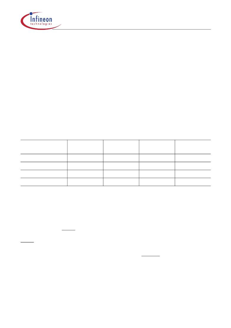
The
frequency
of
these
working
2.048/4.096/8.192/16.384 Mbit/s for the receive and transmit system interface is
programmable by SIC1.SSC1/0, and SIC1.SSD1, FMR1.SSD0. Selectable system clock
and data rates and their valid combinations are shown in the table below
clocks
and
the
data
rate
of
×
= valid, - = invalid
Generally the data or marker on the system interface are clocked off or latched on the
rising or falling edge (SIC3.RESR/X) of the SCLKR/X clock. Some clocking rates allow
transmission of time slots in different channel phases. Each channel phase which shall
be active on ports RDO, XDI, RP(A:D) and XP(A:D) is programmable by SIC2.SICS(2:0),
the remaining channel phases are cleared or ignored.
The signals on pin SYPR together with the assigned time slot offset in register RC0 and
RC1 define the beginning of a frame on the receive system highway.The signal on pin
SYPX or XMFS together with the assigned time slot offset in register XC0 and XC1
define the beginning of a frame on the transmit system highway.
Adjusting the frame begin (time slot 0, bit 0) relative to SYPR/X or XMFS is possible in
the range of 0 to 125 μs. The minimum shift of varying the time slot 0 begin can be
programmed between 1 bit and 1/8 bit depending of the system clocking and data rate,
e.g. with a clocking/data rate of 2.048 MHz shifting is done bit by bit, while running the
FALC
56 with 16.384 MHz and 2.048 Mbit/s data rate it is done by 1/8 bit.
A receive frame marker RFM can be activated during any bit position of the entire frame.
Programming is done with registers RC1/0. The pin function RFM is selected by
Table 24
System Data Rate
System Clocking and Data Rates (E1)
Clock Rate
2.048 MHz
×
-
-
-
Clock Rate
4.096 MHz
×
×
-
-
Clock Rate
8.192 MHz
×
×
×
-
Clock Rate
16.384 MHz
×
×
×
×
2.048 Mbit/s
4.096 Mbit/s
8.192 Mbit/s
16.384 Mbit/s
相关PDF资料 |
PDF描述 |
|---|---|
| PEF22810 | ETHERNET OVER VDSL CHIPSET |
| PEF22822FV22 | ETHERNET OVER VDSL CHIPSET |
| PEF22822ELV22 | ETHERNET OVER VDSL CHIPSET |
| PEB22811HV13 | ETHERNET OVER VDSL CHIPSET |
| PEF22810TV21 | ETHERNET OVER VDSL CHIPSET |
相关代理商/技术参数 |
参数描述 |
|---|---|
| PEF2256H V2.2 | 制造商:Lantiq 功能描述: |
| PEF2256HV2.2 | 功能描述:网络控制器与处理器 IC T/E RoHS:否 制造商:Micrel 产品:Controller Area Network (CAN) 收发器数量: 数据速率: 电源电流(最大值):595 mA 最大工作温度:+ 85 C 安装风格:SMD/SMT 封装 / 箱体:PBGA-400 封装:Tray |
| PEF2256HV22XP | 制造商:Lantiq 功能描述:Framer E1/J1/T1 1.8V/3.3V 80-Pin MQFP |
| PEF2260NV3.0 | 制造商:Infineon Technologies AG 功能描述: |
| PEF2260NV3.0SICOFI | 制造商:Rochester Electronics LLC 功能描述:- Bulk |
发布紧急采购,3分钟左右您将得到回复。