- 您现在的位置:买卖IC网 > PDF目录296941 > QL8150-6PT280I (QUICKLOGIC CORP) FPGA, 640 CLBS, 188946 GATES, PBGA280 PDF资料下载
参数资料
| 型号: | QL8150-6PT280I |
| 厂商: | QUICKLOGIC CORP |
| 元件分类: | FPGA |
| 英文描述: | FPGA, 640 CLBS, 188946 GATES, PBGA280 |
| 封装: | 0.80 MM PITCH, LFBGA-280 |
| 文件页数: | 30/96页 |
| 文件大小: | 1607K |
| 代理商: | QL8150-6PT280I |
第1页第2页第3页第4页第5页第6页第7页第8页第9页第10页第11页第12页第13页第14页第15页第16页第17页第18页第19页第20页第21页第22页第23页第24页第25页第26页第27页第28页第29页当前第30页第31页第32页第33页第34页第35页第36页第37页第38页第39页第40页第41页第42页第43页第44页第45页第46页第47页第48页第49页第50页第51页第52页第53页第54页第55页第56页第57页第58页第59页第60页第61页第62页第63页第64页第65页第66页第67页第68页第69页第70页第71页第72页第73页第74页第75页第76页第77页第78页第79页第80页第81页第82页第83页第84页第85页第86页第87页第88页第89页第90页第91页第92页第93页第94页第95页第96页
2007 QuickLogic Corporation
Eclipse II Family Data Sheet Rev. Q
36
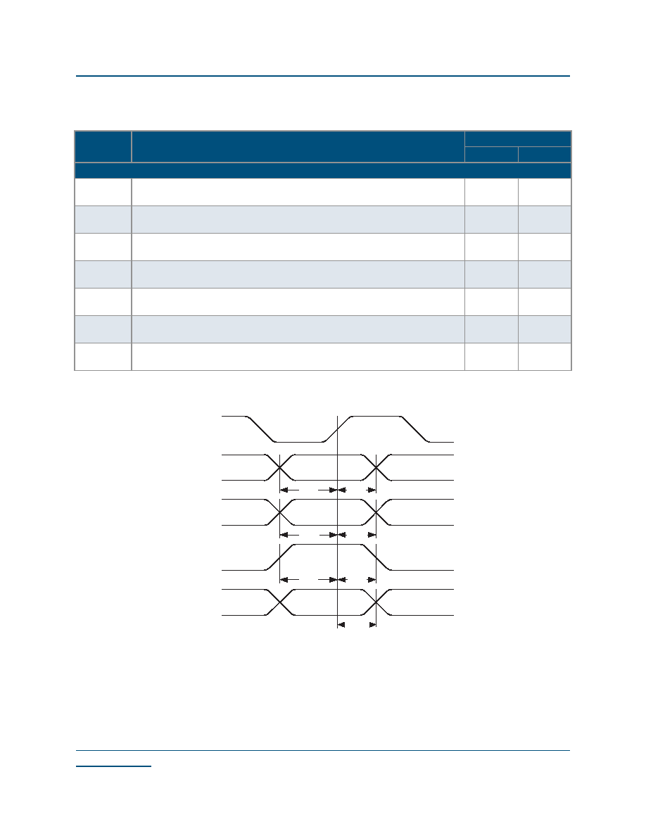
Figure 37: RAM Cell Synchronous Write Timing
Table 22: RAM Cell Synchronous Write Timing
Symbol
Parameter
Value
Min
Max
RAM Cell Synchronous Write Timing
tSWA
WA setup time to WCLK: time the WRITE ADDRESS must be stable before the
active edge of the WRITE CLOCK
0.47 ns
-
t
HWA
WA hold time to WCLK: time the WRITE ADDRESS must be stable after the
active edge of the WRITE CLOCK
0 ns
-
tSWD
WD setup time to WCLK: time the WRITE DATA must be stable before the active
edge of the WRITE CLOCK
0.48 ns
-
tHWD
WD hold time to WCLK: time the WRITE DATA must be stable after the active
edge of the WRITE CLOCK
0 ns
-
t
SWE
WE setup time to WCLK: time the WRITE ENABLE must be stable before the
active edge of the WRITE CLOCK
0 ns
-
tHWE
WE hold time to WCLK: time the WRITE ENABLE must be stable after the active
edge of the WRITE CLOCK
0 ns
-
tWCRD
WCLK to RD (WA = RA): time between the active WRITE CLOCK edge and the
time when the data is available at RD
-
3.79 ns
tSWA
tSWD
tSWE
tHWA
tHWD
tHWE
tWCRD
old data
new data
WCLK
WA
WD
WE
RD
相关PDF资料 |
PDF描述 |
|---|---|
| QL8150-6PT280M | FPGA, 640 CLBS, 188946 GATES, PBGA280 |
| QL8150-6PTN280C | FPGA, 640 CLBS, 188946 GATES, PBGA280 |
| QL8150-6PTN280I | FPGA, 640 CLBS, 188946 GATES, PBGA280 |
| QL8150-6PTN280M | FPGA, 640 CLBS, 188946 GATES, PBGA280 |
| QL8150-6PUN196C | FPGA, 640 CLBS, 188946 GATES, PBGA196 |
相关代理商/技术参数 |
参数描述 |
|---|---|
| QL8250 | 制造商:未知厂家 制造商全称:未知厂家 功能描述:LOW POWER FPGA COMBINING PERFORMANCE DENSITY AND EMBEDED RAM |
| QL8250-6PQN208C-5690 | 制造商:QuickLogic Corporation 功能描述: |
| QL8250-6PQN208C-5691 | 制造商:QuickLogic Corporation 功能描述: |
| QL82SD | 制造商:未知厂家 制造商全称:未知厂家 功能描述:10 High Speed Bus LVDS Serial Links bandwidth up to 5 Gbps |
| QL82SD-PB516 | 制造商:未知厂家 制造商全称:未知厂家 功能描述:10 High Speed Bus LVDS Serial Links bandwidth up to 5 Gbps |
发布紧急采购,3分钟左右您将得到回复。