- 您现在的位置:买卖IC网 > PDF目录296941 > QL8150-6PT280I (QUICKLOGIC CORP) FPGA, 640 CLBS, 188946 GATES, PBGA280 PDF资料下载
参数资料
| 型号: | QL8150-6PT280I |
| 厂商: | QUICKLOGIC CORP |
| 元件分类: | FPGA |
| 英文描述: | FPGA, 640 CLBS, 188946 GATES, PBGA280 |
| 封装: | 0.80 MM PITCH, LFBGA-280 |
| 文件页数: | 39/96页 |
| 文件大小: | 1607K |
| 代理商: | QL8150-6PT280I |
第1页第2页第3页第4页第5页第6页第7页第8页第9页第10页第11页第12页第13页第14页第15页第16页第17页第18页第19页第20页第21页第22页第23页第24页第25页第26页第27页第28页第29页第30页第31页第32页第33页第34页第35页第36页第37页第38页当前第39页第40页第41页第42页第43页第44页第45页第46页第47页第48页第49页第50页第51页第52页第53页第54页第55页第56页第57页第58页第59页第60页第61页第62页第63页第64页第65页第66页第67页第68页第69页第70页第71页第72页第73页第74页第75页第76页第77页第78页第79页第80页第81页第82页第83页第84页第85页第86页第87页第88页第89页第90页第91页第92页第93页第94页第95页第96页
2007 QuickLogic Corporation
Eclipse II Family Data Sheet Rev. Q
44
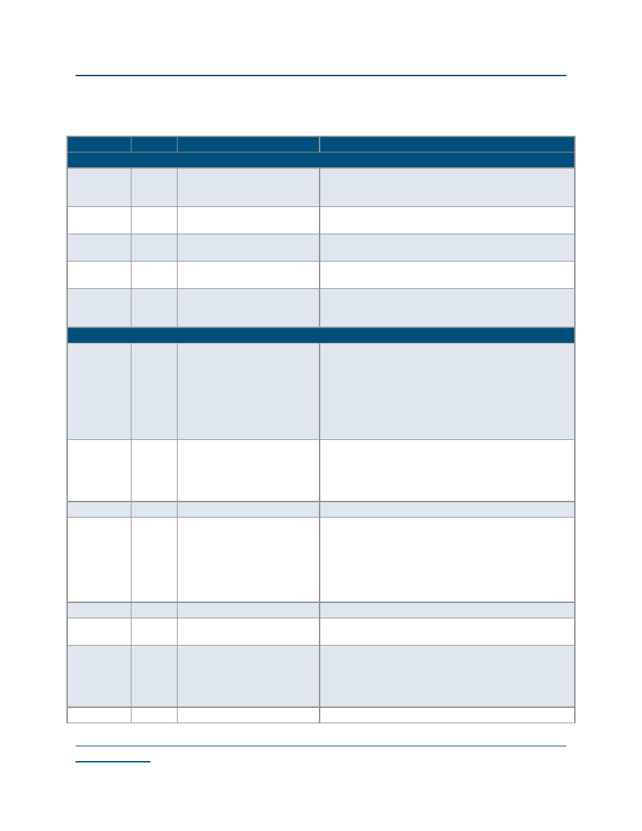
Pin Descriptions
Table 31: Pin Descriptions
Pin
Direction
Function
Description
JTAG Pin Descriptions
TDI/RSI
I
Test Data In for JTAG/RAM init.
Serial Data In
Hold HIGH during normal operation. Connects to serial
PROM data in for RAM initialization. Connect to VDED2 if
unused
TRSTB/RRO
I/0
Active low Reset for JTAG/RAM
init. reset out
Hold LOW during normal operation. Connects to serial
PROM reset for RAM initialization. Connect to GND if unused
TMS
I
Test Mode Select for JTAG
Hold HIGH during normal operation. Connect to VDED2 if not
used for JTAG
TCK
I
Test Clock for JTAG
Hold HIGH or LOW during normal operation. Connect to
VDED2 or GND if not used for JTAG
TDO/RCO
O
Test data out for JTAG/RAM init.
clock out
Connect to serial PROM clock for RAM initialization. Must be
left unconnected if not used for JTAG or RAM initialization.
The output voltage drive is specified by VDED.
Dedicated Pin Descriptions
CLK
I
Global clock network pin
Low skew global clock. This pin provides access to a
dedicated, distributed network capable of driving the CLOCK,
SET, RESET, F1, and A2 inputs to the Logic Cell, READ, and
WRITE CLOCKS, Read and Write Enables of the Embedded
RAM Blocks, CLOCK of the ECUs, and Output Enables of the
I/Os. The voltage tolerance of this pin is specified by VDED.
The voltage tolerance of the CLK pins in the PU101
package are specified by VCCIO(B).
I/O(A)
I/O
Input/Output pin
The I/O pin is a bi-directional pin, configurable to either an
input-only, output-only, or bi-directional pin. The A inside the
parenthesis means that the I/O is located in Bank A. If an I/O
is not used, SpDE (QuickWorks Tool) provides the option of
tying that pin to GND, VCC
, or TriState.
VCC
I
Power supply pin
Connect to 1.8 V supply.
VCCIO(A)
I
Input voltage tolerance pin
This pin provides the flexibility to interface the device with
either a 3.3 V, 2.5 V, or 1.8 V device. The A inside the
parenthesis means that VCCIO is located in BANK A. Every
I/O pin in Bank A will be tolerant of VCCIO input signals and
will drive VCCIO level output signals. This pin must be
connected to either 3.3 V, 2.5 V, or 1.8 V. VCCIO powers the
the PLLOUT pins.
GND
I
Ground pin
Connect to ground.
PLLIN
I
PLL clock input
Clock input for PLL. The voltage tolerance of this pin is
specified by VDED.
DEDCLK
I
Dedicated clock pin
Very low skew global clock. This pin provides access to a
dedicated, distributed clock network capable of driving the
CLOCK inputs of all sequential elements of the device (e.g.,
RAM, Flip Flops). The voltage tolerance of this pin is
specified by VDED.
GNDPLL
I
Ground pin for PLL
Connect to GND.
相关PDF资料 |
PDF描述 |
|---|---|
| QL8150-6PT280M | FPGA, 640 CLBS, 188946 GATES, PBGA280 |
| QL8150-6PTN280C | FPGA, 640 CLBS, 188946 GATES, PBGA280 |
| QL8150-6PTN280I | FPGA, 640 CLBS, 188946 GATES, PBGA280 |
| QL8150-6PTN280M | FPGA, 640 CLBS, 188946 GATES, PBGA280 |
| QL8150-6PUN196C | FPGA, 640 CLBS, 188946 GATES, PBGA196 |
相关代理商/技术参数 |
参数描述 |
|---|---|
| QL8250 | 制造商:未知厂家 制造商全称:未知厂家 功能描述:LOW POWER FPGA COMBINING PERFORMANCE DENSITY AND EMBEDED RAM |
| QL8250-6PQN208C-5690 | 制造商:QuickLogic Corporation 功能描述: |
| QL8250-6PQN208C-5691 | 制造商:QuickLogic Corporation 功能描述: |
| QL82SD | 制造商:未知厂家 制造商全称:未知厂家 功能描述:10 High Speed Bus LVDS Serial Links bandwidth up to 5 Gbps |
| QL82SD-PB516 | 制造商:未知厂家 制造商全称:未知厂家 功能描述:10 High Speed Bus LVDS Serial Links bandwidth up to 5 Gbps |
发布紧急采购,3分钟左右您将得到回复。