- 您现在的位置:买卖IC网 > PDF目录296941 > QL8150-6PT280I (QUICKLOGIC CORP) FPGA, 640 CLBS, 188946 GATES, PBGA280 PDF资料下载
参数资料
| 型号: | QL8150-6PT280I |
| 厂商: | QUICKLOGIC CORP |
| 元件分类: | FPGA |
| 英文描述: | FPGA, 640 CLBS, 188946 GATES, PBGA280 |
| 封装: | 0.80 MM PITCH, LFBGA-280 |
| 文件页数: | 45/96页 |
| 文件大小: | 1607K |
| 代理商: | QL8150-6PT280I |
第1页第2页第3页第4页第5页第6页第7页第8页第9页第10页第11页第12页第13页第14页第15页第16页第17页第18页第19页第20页第21页第22页第23页第24页第25页第26页第27页第28页第29页第30页第31页第32页第33页第34页第35页第36页第37页第38页第39页第40页第41页第42页第43页第44页当前第45页第46页第47页第48页第49页第50页第51页第52页第53页第54页第55页第56页第57页第58页第59页第60页第61页第62页第63页第64页第65页第66页第67页第68页第69页第70页第71页第72页第73页第74页第75页第76页第77页第78页第79页第80页第81页第82页第83页第84页第85页第86页第87页第88页第89页第90页第91页第92页第93页第94页第95页第96页
2007 QuickLogic Corporation
Eclipse II Family Data Sheet Rev. Q
5
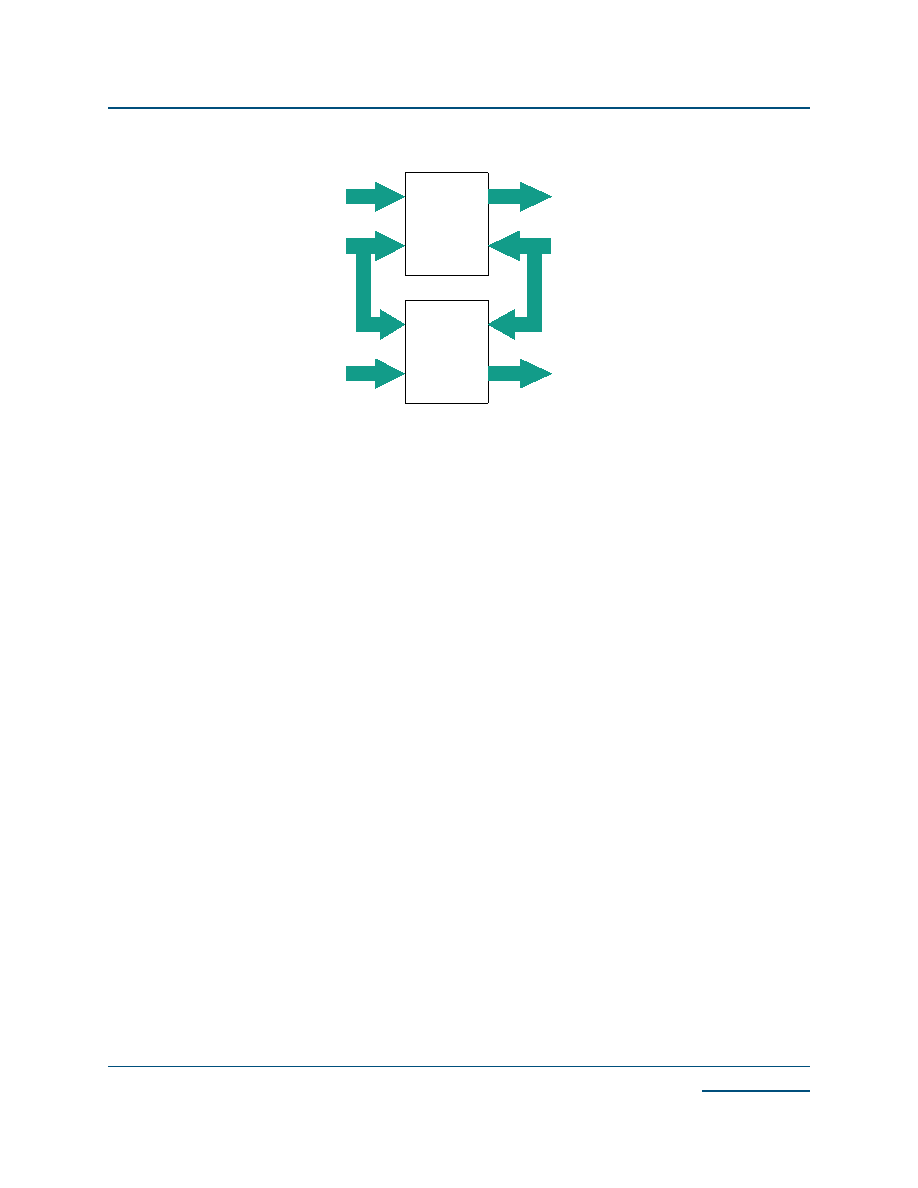
Figure 4: Cascaded RAM Modules
The RAM modules are dual-port, with completely independent READ and WRITE ports and separate READ
and WRITE clocks. The READ ports support asynchronous and synchronous operation, while the WRITE
ports support synchronous operation. Each port has 18 data lines and 8 address lines, allowing word lengths
of up to 18 bits and address spaces of up to 256 words. Depending on the mode selected, however, some
higher order data or address lines may not be used.
The Write Enable (WE) line acts as a clock enable for synchronous write operation. The Read Enable (RE) acts
as a clock enable for synchronous READ operation (ASYNCRD input low), or as a flow-through enable for
asynchronous READ operation (ASYNCRD input high).
Designers can cascade multiple RAM modules to increase the depth or width allowed in single modules by
connecting corresponding address lines together and dividing the words between modules.
A similar technique can be used to create depths greater than 256 words. In this case address signals higher
than the MSB are encoded onto the write enable (WE) input for WRITE operations. The READ data outputs
are multiplexed together using encoded higher READ address bits for the multiplexer SELECT signals.
The RAM blocks can be loaded with data generated internally (typically for RAM or FIFO functions) or with
data from an external PROM (typically for ROM functions).
Embedded Computational Unit (ECU)
Traditional Programmable Logic architectures do not implement arithmetic functions efficiently or effectively—
these functions require high logic cell usage while garnering only moderate performance results.
The Eclipse II architecture allows for functionality above and beyond that achievable using programmable logic
devices. By embedding a dynamically reconfigurable computational unit, the Eclipse II device can address
various arithmetic functions efficiently. This approach offers greater performance and utilization than
traditional programmable logic implementations. The embedded block is implemented at the transistor level
as shown in Figure 5.
WDATA
RDATA
WADDR
WDATA
RADDR
RAM
Module
(2,304 bits)
RAM
Module
(2,304 bits)
相关PDF资料 |
PDF描述 |
|---|---|
| QL8150-6PT280M | FPGA, 640 CLBS, 188946 GATES, PBGA280 |
| QL8150-6PTN280C | FPGA, 640 CLBS, 188946 GATES, PBGA280 |
| QL8150-6PTN280I | FPGA, 640 CLBS, 188946 GATES, PBGA280 |
| QL8150-6PTN280M | FPGA, 640 CLBS, 188946 GATES, PBGA280 |
| QL8150-6PUN196C | FPGA, 640 CLBS, 188946 GATES, PBGA196 |
相关代理商/技术参数 |
参数描述 |
|---|---|
| QL8250 | 制造商:未知厂家 制造商全称:未知厂家 功能描述:LOW POWER FPGA COMBINING PERFORMANCE DENSITY AND EMBEDED RAM |
| QL8250-6PQN208C-5690 | 制造商:QuickLogic Corporation 功能描述: |
| QL8250-6PQN208C-5691 | 制造商:QuickLogic Corporation 功能描述: |
| QL82SD | 制造商:未知厂家 制造商全称:未知厂家 功能描述:10 High Speed Bus LVDS Serial Links bandwidth up to 5 Gbps |
| QL82SD-PB516 | 制造商:未知厂家 制造商全称:未知厂家 功能描述:10 High Speed Bus LVDS Serial Links bandwidth up to 5 Gbps |
发布紧急采购,3分钟左右您将得到回复。