- 您现在的位置:买卖IC网 > PDF目录296941 > QL8150-6PT280I (QUICKLOGIC CORP) FPGA, 640 CLBS, 188946 GATES, PBGA280 PDF资料下载
参数资料
| 型号: | QL8150-6PT280I |
| 厂商: | QUICKLOGIC CORP |
| 元件分类: | FPGA |
| 英文描述: | FPGA, 640 CLBS, 188946 GATES, PBGA280 |
| 封装: | 0.80 MM PITCH, LFBGA-280 |
| 文件页数: | 43/96页 |
| 文件大小: | 1607K |
| 代理商: | QL8150-6PT280I |
第1页第2页第3页第4页第5页第6页第7页第8页第9页第10页第11页第12页第13页第14页第15页第16页第17页第18页第19页第20页第21页第22页第23页第24页第25页第26页第27页第28页第29页第30页第31页第32页第33页第34页第35页第36页第37页第38页第39页第40页第41页第42页当前第43页第44页第45页第46页第47页第48页第49页第50页第51页第52页第53页第54页第55页第56页第57页第58页第59页第60页第61页第62页第63页第64页第65页第66页第67页第68页第69页第70页第71页第72页第73页第74页第75页第76页第77页第78页第79页第80页第81页第82页第83页第84页第85页第86页第87页第88页第89页第90页第91页第92页第93页第94页第95页第96页
2007 QuickLogic Corporation
Eclipse II Family Data Sheet Rev. Q
48
Recommended Unused Pin Terminations for Eclipse II Devices
All unused, general purpose I/O pins can be tied to VCC, GND, or HIZ (high impedance) internally using the
Configuration Editor. This option is given in the bottom-right corner of the placement window. To use the
Placement Editor, choose Constraint
> Fix Placement in the Option pull-down menu of SpDE.
The rest of the pins should be terminated at the board level in the manner presented in Table 33.
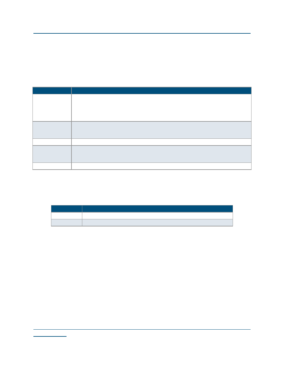
Table 33: Recommended Unused Pin Terminations
Signal Name
Recommended Termination
PLLOUT<x>a
a. x represents a number.
In earlier versions, the recommendation for unused PLLOUT pins was that they be connected to
VCC or GND. This was acceptable for Rev. D (and earlier) silicon, including all 0.25 m devices.
For Rev. G (and later) silicon this is not correct. Unused PLLOUT pins should be left unconnected.
Used PLLOUT pins will normally be connected to inputs, but can also be left unconnected. For the
truth table of PLLOUT connections, refer to
IOCTRL<y>b
b. y represents an alphabetical character.
There is an internal pulldown resistor to GND on this pin. This pin should be tied to GND if it is not
used. For backwards compatibility with Eclipse, it can be tied to VDED or GND. If tied to VDED, it
will draw no more than 20 A per IOCTRL pin due to current through the pulldown resistor.
CLK/PLLIN<x>
Any unused clock pins should be connected to VDED or GND.
PLLRST<x>
If a PLL module is not used, then the associated PLLRST<x> must be connected to VDED or GND.
If VCCPLL is grounded, then PLLRST must be grounded also. If VCCPLL is driven by 2.5 V or
3.3 V, PLLRST must be driven by the same voltage.
INREF<y>
If an I/O bank does not require the use of the INREF signal the pin should be connected to GND.
Table 34: Recommended PLLOUT Terminations Truth Table
PLL_RESET
Recommended PLLOUT Termination
0
Must be left unconnected.
1
May be left unconnected, or connected to GND. Must not be connected to VCC.
相关PDF资料 |
PDF描述 |
|---|---|
| QL8150-6PT280M | FPGA, 640 CLBS, 188946 GATES, PBGA280 |
| QL8150-6PTN280C | FPGA, 640 CLBS, 188946 GATES, PBGA280 |
| QL8150-6PTN280I | FPGA, 640 CLBS, 188946 GATES, PBGA280 |
| QL8150-6PTN280M | FPGA, 640 CLBS, 188946 GATES, PBGA280 |
| QL8150-6PUN196C | FPGA, 640 CLBS, 188946 GATES, PBGA196 |
相关代理商/技术参数 |
参数描述 |
|---|---|
| QL8250 | 制造商:未知厂家 制造商全称:未知厂家 功能描述:LOW POWER FPGA COMBINING PERFORMANCE DENSITY AND EMBEDED RAM |
| QL8250-6PQN208C-5690 | 制造商:QuickLogic Corporation 功能描述: |
| QL8250-6PQN208C-5691 | 制造商:QuickLogic Corporation 功能描述: |
| QL82SD | 制造商:未知厂家 制造商全称:未知厂家 功能描述:10 High Speed Bus LVDS Serial Links bandwidth up to 5 Gbps |
| QL82SD-PB516 | 制造商:未知厂家 制造商全称:未知厂家 功能描述:10 High Speed Bus LVDS Serial Links bandwidth up to 5 Gbps |
发布紧急采购,3分钟左右您将得到回复。