- 您现在的位置:买卖IC网 > PDF目录296941 > QL8150-6PT280I (QUICKLOGIC CORP) FPGA, 640 CLBS, 188946 GATES, PBGA280 PDF资料下载
参数资料
| 型号: | QL8150-6PT280I |
| 厂商: | QUICKLOGIC CORP |
| 元件分类: | FPGA |
| 英文描述: | FPGA, 640 CLBS, 188946 GATES, PBGA280 |
| 封装: | 0.80 MM PITCH, LFBGA-280 |
| 文件页数: | 89/96页 |
| 文件大小: | 1607K |
| 代理商: | QL8150-6PT280I |
第1页第2页第3页第4页第5页第6页第7页第8页第9页第10页第11页第12页第13页第14页第15页第16页第17页第18页第19页第20页第21页第22页第23页第24页第25页第26页第27页第28页第29页第30页第31页第32页第33页第34页第35页第36页第37页第38页第39页第40页第41页第42页第43页第44页第45页第46页第47页第48页第49页第50页第51页第52页第53页第54页第55页第56页第57页第58页第59页第60页第61页第62页第63页第64页第65页第66页第67页第68页第69页第70页第71页第72页第73页第74页第75页第76页第77页第78页第79页第80页第81页第82页第83页第84页第85页第86页第87页第88页当前第89页第90页第91页第92页第93页第94页第95页第96页
2007 QuickLogic Corporation
Eclipse II Family Data Sheet Rev. Q
9
PLL Signals
Table 7 summarizes the key signals in QuickLogic PLLs.
NOTE: Because PLLCLK_IN and PLL_RESET signals have PLL_INPAD, and PLLPAD_OUT has OUTPAD,
you do not need to add additional pads to your design.
I/O Cell Structure
Eclipse II features a variety of distinct I/O pins to maximize performance, functionality, and flexibility with bi-
directional I/O pins and input-only pins. All input and I/O pins are 1.8 V, 2.5 V, and 3.3 V tolerant and comply
with the specific I/O standard selected. For single ended I/O standards, VCCIO specifies the input tolerance
and the output drive. For voltage referenced I/O standards (e.g SSTL), the voltage supplied to the INREF pins
in each bank specifies the input switch point. For example, the VCCIO pins must be tied to a 3.3 V supply to
provide 3.3 V compliance. Eclipse II can also support the LVDS and LVPECL I/O standards with the use of
external resistors (see Table 8).
As designs become more complex and requirements more stringent, several application-specific I/O standards
have emerged for specific applications. I/O standards for processors, memories, and a variety of bus
applications have become commonplace and a requirement for many systems. In addition, I/O timing has
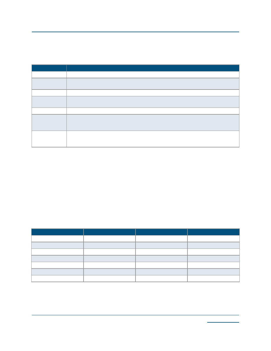
Table 7: QuickLogic PLL Signals
Signal Name
Description
PLLCLK_IN
Input clock signal.
PLL_RESET
Active High Reset If PLL_RESET is asserted, then CLKNET_OUT and PLLPAD_OUT are reset
to 0. This signal must be asserted and then released in order for the LOCK_DETECT to work.
ONn_OFFCHIP
This is a reserved signal. It can be connected to VCC or GND.
CLKNET_OUT
Out to internal gates This signal bypasses the PLL logic before driving the clock tree. Note that
this signal cannot be used in the same quadrant where the PLL signal is used (PLLCLK_OUT).
PLLCLK_OUT
Out from PLL to internal gates This signal can drive the clock tree after going through the PLL.
PLLPAD_OUT
Out to off-chip This outgoing signal is used off-chip. The PLLPAD_OUT is always active, driving
the PLL-derived clock signal out through the pad. The PLLPAD_OUT will not oscillate if
PLL_RESET is asserted, or if the PLL is powered down.
LOCK_DETECT
Active High Lock detection signal
NOTE: For simulation purposes, this signal gets asserted after 10 clock cycles. However, it can take
a maximum of 200 clock cycles to sync with the input clock upon release of the PLL_RESET signal.
Table 8: I/O Standards and Applications
I/O Standard
Reference Voltage
Output Voltage
Application
LVTTL
n/a
3.3 V
General Purpose
LVCMOS25
n/a
2.5 V
General Purpose
LVCMOS18
n/a
1.8 V
General Purpose
PCI
n/a
3.3 V
PCI Bus Applications
GTL+
1
n/a
Backplane
SSTL3
1.5
3.3 V
SDRAM
SSTL2
1.25
2.5 V
SDRAM
相关PDF资料 |
PDF描述 |
|---|---|
| QL8150-6PT280M | FPGA, 640 CLBS, 188946 GATES, PBGA280 |
| QL8150-6PTN280C | FPGA, 640 CLBS, 188946 GATES, PBGA280 |
| QL8150-6PTN280I | FPGA, 640 CLBS, 188946 GATES, PBGA280 |
| QL8150-6PTN280M | FPGA, 640 CLBS, 188946 GATES, PBGA280 |
| QL8150-6PUN196C | FPGA, 640 CLBS, 188946 GATES, PBGA196 |
相关代理商/技术参数 |
参数描述 |
|---|---|
| QL8250 | 制造商:未知厂家 制造商全称:未知厂家 功能描述:LOW POWER FPGA COMBINING PERFORMANCE DENSITY AND EMBEDED RAM |
| QL8250-6PQN208C-5690 | 制造商:QuickLogic Corporation 功能描述: |
| QL8250-6PQN208C-5691 | 制造商:QuickLogic Corporation 功能描述: |
| QL82SD | 制造商:未知厂家 制造商全称:未知厂家 功能描述:10 High Speed Bus LVDS Serial Links bandwidth up to 5 Gbps |
| QL82SD-PB516 | 制造商:未知厂家 制造商全称:未知厂家 功能描述:10 High Speed Bus LVDS Serial Links bandwidth up to 5 Gbps |
发布紧急采购,3分钟左右您将得到回复。