- 您现在的位置:买卖IC网 > PDF目录296941 > QL8150-6PT280I (QUICKLOGIC CORP) FPGA, 640 CLBS, 188946 GATES, PBGA280 PDF资料下载
参数资料
| 型号: | QL8150-6PT280I |
| 厂商: | QUICKLOGIC CORP |
| 元件分类: | FPGA |
| 英文描述: | FPGA, 640 CLBS, 188946 GATES, PBGA280 |
| 封装: | 0.80 MM PITCH, LFBGA-280 |
| 文件页数: | 8/96页 |
| 文件大小: | 1607K |
| 代理商: | QL8150-6PT280I |
第1页第2页第3页第4页第5页第6页第7页当前第8页第9页第10页第11页第12页第13页第14页第15页第16页第17页第18页第19页第20页第21页第22页第23页第24页第25页第26页第27页第28页第29页第30页第31页第32页第33页第34页第35页第36页第37页第38页第39页第40页第41页第42页第43页第44页第45页第46页第47页第48页第49页第50页第51页第52页第53页第54页第55页第56页第57页第58页第59页第60页第61页第62页第63页第64页第65页第66页第67页第68页第69页第70页第71页第72页第73页第74页第75页第76页第77页第78页第79页第80页第81页第82页第83页第84页第85页第86页第87页第88页第89页第90页第91页第92页第93页第94页第95页第96页
2007 QuickLogic Corporation
Eclipse II Family Data Sheet Rev. Q
16
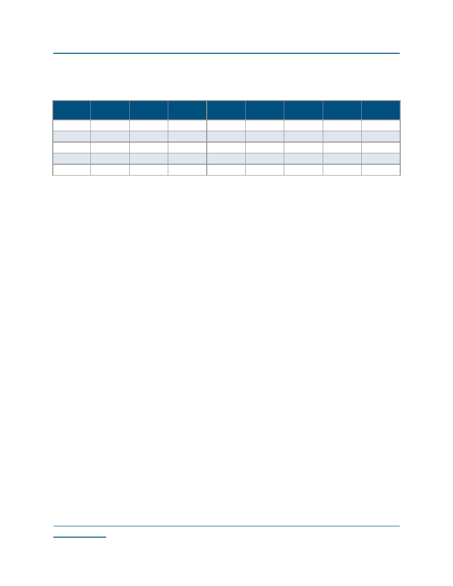
Table 10 shows the total number of I/O control pins per device/package combination. These pins are not
bonded out in the smaller devices and packages. This increases the number of bi-directional user I/Os available.
Programmable Logic Routing
Eclipse II devices are engineered with six types of routing resources as follows: short (sometimes called
segmented) wires, dual wires, quad wires, express wires, distributed networks, and default wires. Short wires
span the length of one logic cell, always in the vertical direction. Dual wires run horizontally and span the
length of two logic cells. Short and dual wires are predominantly used for local connections. Default wires
supply VCC and GND (Logic ‘1’ and Logic ‘0’) to each column of logic cells.
Quad wires have passive link interconnect elements every fourth logic cell. As a result, these wires are typically
used to implement intermediate length or medium fan-out nets.
Express lines run the length of the device, uninterrupted. Each of these lines has a higher capacitance than a
quad, dual, or short wire, but less capacitance than shorter wires connected to run the length of the device.
The resistance will also be lower because the express wires don't require the use of pass links. Express wires
provide higher performance for long routes or high fan-out nets.
Distributed networks are described in Clock Networks on page 14. These wires span the programmable logic
and are driven by quad-net buffers.
Global Power-On Reset (POR)
The Eclipse II family of devices features a global power-on reset. This reset is hardwired to all registers and
resets them to Logic ‘0’ upon power-up of the device. In QuickLogic devices, the asynchronous Reset input
to flip-flops has priority over the Set input; therefore, the Global POR will reset all flip-flops during power-up.
If you want to set the flip-flops to Logic ‘1’, you must assert the “Set” signal after the Global POR signal has
been deasserted.
Table 10: I/O Control Pins per Device/Package Combination
Device
100 VQFP
101
CTBGA
144 TQFP
196 TFBGA
(0.8 mm)
196 TFBGA
(0.5 mm)
208 PQFP 280 LFBGA
484 BGA
QL8025
-
NA
-
NAa
a. Not available.
NA
QL8050
-
NA
QL8150
NA
-
NA
QL8250
NA
-
16
QL8325
NA
-
16
相关PDF资料 |
PDF描述 |
|---|---|
| QL8150-6PT280M | FPGA, 640 CLBS, 188946 GATES, PBGA280 |
| QL8150-6PTN280C | FPGA, 640 CLBS, 188946 GATES, PBGA280 |
| QL8150-6PTN280I | FPGA, 640 CLBS, 188946 GATES, PBGA280 |
| QL8150-6PTN280M | FPGA, 640 CLBS, 188946 GATES, PBGA280 |
| QL8150-6PUN196C | FPGA, 640 CLBS, 188946 GATES, PBGA196 |
相关代理商/技术参数 |
参数描述 |
|---|---|
| QL8250 | 制造商:未知厂家 制造商全称:未知厂家 功能描述:LOW POWER FPGA COMBINING PERFORMANCE DENSITY AND EMBEDED RAM |
| QL8250-6PQN208C-5690 | 制造商:QuickLogic Corporation 功能描述: |
| QL8250-6PQN208C-5691 | 制造商:QuickLogic Corporation 功能描述: |
| QL82SD | 制造商:未知厂家 制造商全称:未知厂家 功能描述:10 High Speed Bus LVDS Serial Links bandwidth up to 5 Gbps |
| QL82SD-PB516 | 制造商:未知厂家 制造商全称:未知厂家 功能描述:10 High Speed Bus LVDS Serial Links bandwidth up to 5 Gbps |
发布紧急采购,3分钟左右您将得到回复。