- 您现在的位置:买卖IC网 > PDF目录385871 > ST7285C (意法半导体) 8-BIT MCU FOR RDS WITH 48K ROM, 3K RAM, ADC, TWO TIMERS, TWO SPIs, I2C AND SCI INTERFACES PDF资料下载
参数资料
| 型号: | ST7285C |
| 厂商: | 意法半导体 |
| 英文描述: | 8-BIT MCU FOR RDS WITH 48K ROM, 3K RAM, ADC, TWO TIMERS, TWO SPIs, I2C AND SCI INTERFACES |
| 中文描述: | 8位微控制器48,000铁路发展策略光盘,3K内存,ADC,两个定时器,2个SPI,I2C和脊髓损伤接口 |
| 文件页数: | 50/117页 |
| 文件大小: | 748K |
| 代理商: | ST7285C |
第1页第2页第3页第4页第5页第6页第7页第8页第9页第10页第11页第12页第13页第14页第15页第16页第17页第18页第19页第20页第21页第22页第23页第24页第25页第26页第27页第28页第29页第30页第31页第32页第33页第34页第35页第36页第37页第38页第39页第40页第41页第42页第43页第44页第45页第46页第47页第48页第49页当前第50页第51页第52页第53页第54页第55页第56页第57页第58页第59页第60页第61页第62页第63页第64页第65页第66页第67页第68页第69页第70页第71页第72页第73页第74页第75页第76页第77页第78页第79页第80页第81页第82页第83页第84页第85页第86页第87页第88页第89页第90页第91页第92页第93页第94页第95页第96页第97页第98页第99页第100页第101页第102页第103页第104页第105页第106页第107页第108页第109页第110页第111页第112页第113页第114页第115页第116页第117页
50/117
ST7285C
SERIAL PERIPHERAL INTERFACE
(Cont’d)
4.4.7 Serial Peripheral Control Register (SPCR)
Address: see Memory Map
Reset Value: 0Xh
—
Read/Write
The Serial Peripheral Control Register bits are de-
fined as follows.
Bit-7 =
SPIE
Serial Peripheral Interrupt Enable
When the Serial Peripheral Interrupts Enable bit is
seta processor interrupt can occur. This forces the
proper vector to be loaded into the program coun-
ter if the Serial Peripheral Status Register flag bit
(SPIF) and /or MODF are set. SPIE does not inhib-
it the setting of a status bit. The SPIE bit is cleared
on Reset.
Bit-6 =
SPE
Serial Peripheral output Enalble
When the Serial Peripheral Output Enable Control
bit is set, all output drive is applied to the external
pins and the system is enabled. When the SPE bit
is set, it enables the SPI system by connecting itto
the external pins thus allowing it to interface with
the external SPI bus. The pins that are defined as
outputs depend on which mode (Master or Slave)
the device is in. Because the SPE bit is cleared on
Reset, the SPI system is not connected to the ex-
ternal pins on Reset.
Bit-4 =
MSTR
Master
The Master bit determines whether the device is a
Master or a Slave. If the MSTR bit is reset it indi-
cates a Slave device, whent it is set it indicates a
Master device. If the Master mode is selected, the
function of the SCK pin changes from an input to
an output and the function of the MISO and MOSI
pins are reversed. This allows the user to wire de-
vice pins MISO to MOSI, and MOSI to MOSI, and
SCK to SCK without incident. The MSTR bit is
cleared on Reset: thus the device is always set in
Slave mode during Reset.
Bit-3 =
CPOL
Clock POLarity
The Clock POLarity bit controls the normal or
steady state value of the clock when no data is be-
ing transferred. The CPOL bit affects both the
Master and Slave modes. It must be used in con-
junction with the Clock PHAse control bit (CPHA)
to produce the wanted clock-data relationship be-
tween a Master and a Slave device. When the
CP0L bit is reset, it produces a steady-state logic
low value on the SCK pin of the Master device. If
the CPOL bit is set, a logic high level is present on
the SCK pin of the Master device when data is not
being transferred. The CPOL bit is not affected by
Reset.
Bit-2 =
CPHA
Clock PHAse
The Clock PHAse bit controls the relationship be-
tween the data on the MISO and MOSI pins and
the clock produced or received at the SCK pin.
This control has effect in both the Master or Slave
modes. It must be used in conjunction with the
Clock Polarity control bit (CPOL) to produce the
wanted clock-data relationship. In general the
CPHA bit selects the clock edge which captures
data and allows it to change states. It has itsgreat-
est impact on the first bit transmitted (MSB) in that
it does or does not allow a clock transition before
the first data capture edge. The CPHA bit is not af-
fected by Reset.
Bit-1 =
SPR1
Serial Peripheral Rate bit 1
Bit-0 =
SPR0
Serial Peripheral Rate bit 0
These two Serial Peripheral Rate bits select one of
four baud rates to be used for SCK when the de-
vice is a Master. However, these two bits have no
effect in Slave mode. The Slave device is capable
of shifting data in and out at a maximum rate which
is equal to the CPU clock. A rate table is given be-
low for SCK inMaster mode. The SPR1 and SPR0
bits are not affected by Reset.
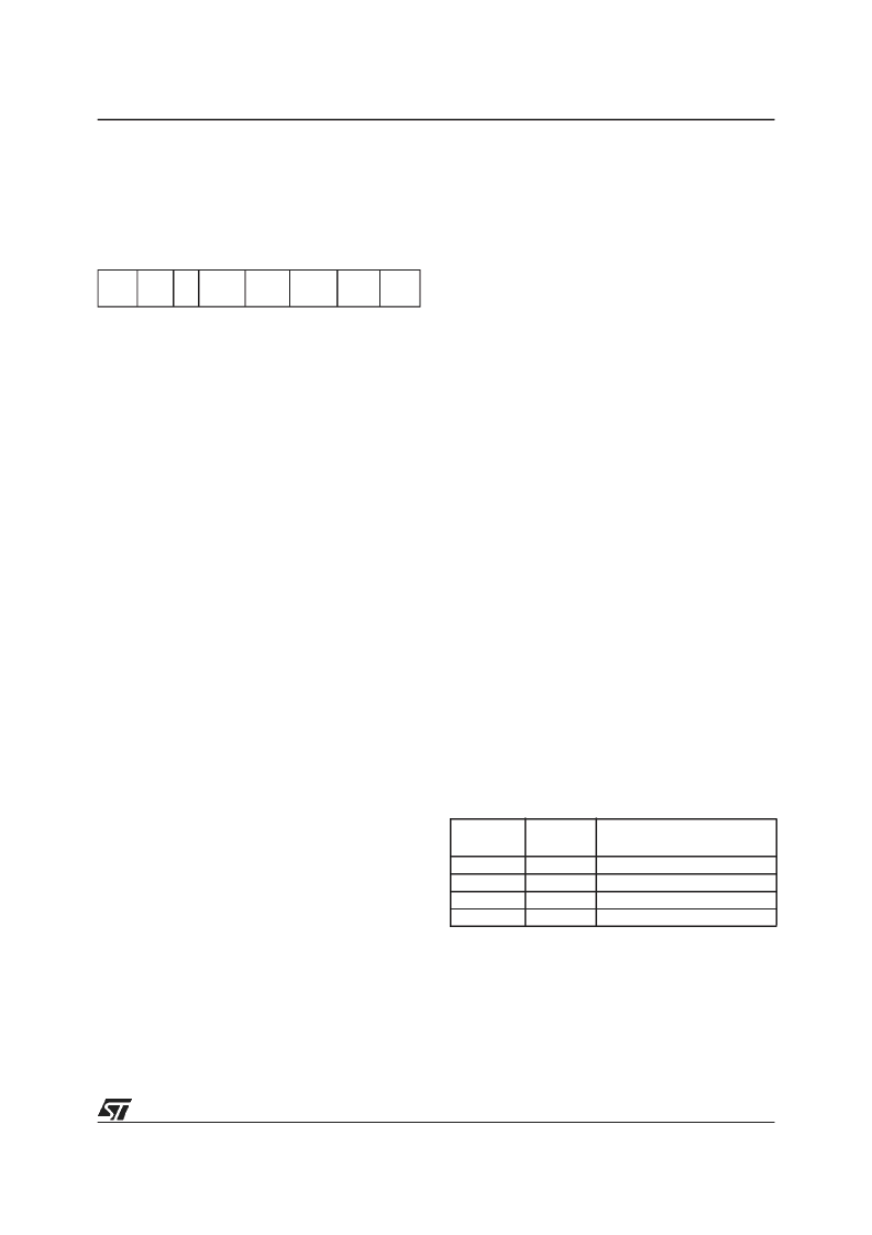
7
0
SPIE
SPE
-
MSTR
CPOL
CPHA
SPR1
SPR0
SPR1
SPR0
Internal Processor
Clock Division factor
2
4
16
32
0
0
1
1
0
1
0
1
相关PDF资料 |
PDF描述 |
|---|---|
| ST72T85A5Q6 | 8-BIT MCU FOR RDS WITH 48K ROM, 3K RAM, ADC, TWO TIMERS, TWO SPIs, I2C AND SCI INTERFACES |
| ST730C08L3 | PHASE CONTROL THYRISTORS |
| ST730C08L3L | PHASE CONTROL THYRISTORS |
| ST730C12L0 | PHASE CONTROL THYRISTORS |
| ST730C12L0L | PHASE CONTROL THYRISTORS |
相关代理商/技术参数 |
参数描述 |
|---|---|
| ST7-28B56 | 功能描述:电源变压器 SPLIT BOBBIN HORZ MOUNT XFMR RoHS:否 制造商:Triad Magnetics 功率额定值:12 VA 初级电压额定值:115 V / 230 V 次级电压额定值:12 V / 24 V 安装风格:SMD/SMT 一次绕组:Dual Primary Winding 二次绕组:Dual Secondary Winding 长度:2.5 in 宽度:2 in 高度:1.062 in |
| ST72A | 制造商:DGS 功能描述: |
| ST72C104G1B6 | 功能描述:8位微控制器 -MCU Flash 4K SPI RoHS:否 制造商:Silicon Labs 核心:8051 处理器系列:C8051F39x 数据总线宽度:8 bit 最大时钟频率:50 MHz 程序存储器大小:16 KB 数据 RAM 大小:1 KB 片上 ADC:Yes 工作电源电压:1.8 V to 3.6 V 工作温度范围:- 40 C to + 105 C 封装 / 箱体:QFN-20 安装风格:SMD/SMT |
| ST72C104G1M1 | 制造商:STMicroelectronics 功能描述:8-BIT MICROCONTROLLER - Bulk |
| ST72C104G1M6 | 功能描述:8位微控制器 -MCU Flash 4K SPI RoHS:否 制造商:Silicon Labs 核心:8051 处理器系列:C8051F39x 数据总线宽度:8 bit 最大时钟频率:50 MHz 程序存储器大小:16 KB 数据 RAM 大小:1 KB 片上 ADC:Yes 工作电源电压:1.8 V to 3.6 V 工作温度范围:- 40 C to + 105 C 封装 / 箱体:QFN-20 安装风格:SMD/SMT |
发布紧急采购,3分钟左右您将得到回复。