- 您现在的位置:买卖IC网 > PDF目录17297 > TMDXBDKFP5515 (Texas Instruments)KIT DEV FINGERPRINT C5515 PDF资料下载
参数资料
| 型号: | TMDXBDKFP5515 |
| 厂商: | Texas Instruments |
| 文件页数: | 42/159页 |
| 文件大小: | 0K |
| 描述: | KIT DEV FINGERPRINT C5515 |
| 标准包装: | 1 |
| 传感器类型: | 指纹 |
| 接口: | USB |
| 电源电压: | 5V |
| 嵌入式: | 是,MCU,16 位 |
| 已供物品: | 板,扩展板,线缆,迷你型 DVD,传感器 |
| 已用 IC / 零件: | C5515 |
| 产品目录页面: | 718 (CN2011-ZH PDF) |
| 其它名称: | 296-27452 |
第1页第2页第3页第4页第5页第6页第7页第8页第9页第10页第11页第12页第13页第14页第15页第16页第17页第18页第19页第20页第21页第22页第23页第24页第25页第26页第27页第28页第29页第30页第31页第32页第33页第34页第35页第36页第37页第38页第39页第40页第41页当前第42页第43页第44页第45页第46页第47页第48页第49页第50页第51页第52页第53页第54页第55页第56页第57页第58页第59页第60页第61页第62页第63页第64页第65页第66页第67页第68页第69页第70页第71页第72页第73页第74页第75页第76页第77页第78页第79页第80页第81页第82页第83页第84页第85页第86页第87页第88页第89页第90页第91页第92页第93页第94页第95页第96页第97页第98页第99页第100页第101页第102页第103页第104页第105页第106页第107页第108页第109页第110页第111页第112页第113页第114页第115页第116页第117页第118页第119页第120页第121页第122页第123页第124页第125页第126页第127页第128页第129页第130页第131页第132页第133页第134页第135页第136页第137页第138页第139页第140页第141页第142页第143页第144页第145页第146页第147页第148页第149页第150页第151页第152页第153页第154页第155页第156页第157页第158页第159页
�� ��
��
��SPRS645F� –� AUGUST� 2010� –� REVISED� OCTOBER� 2013�
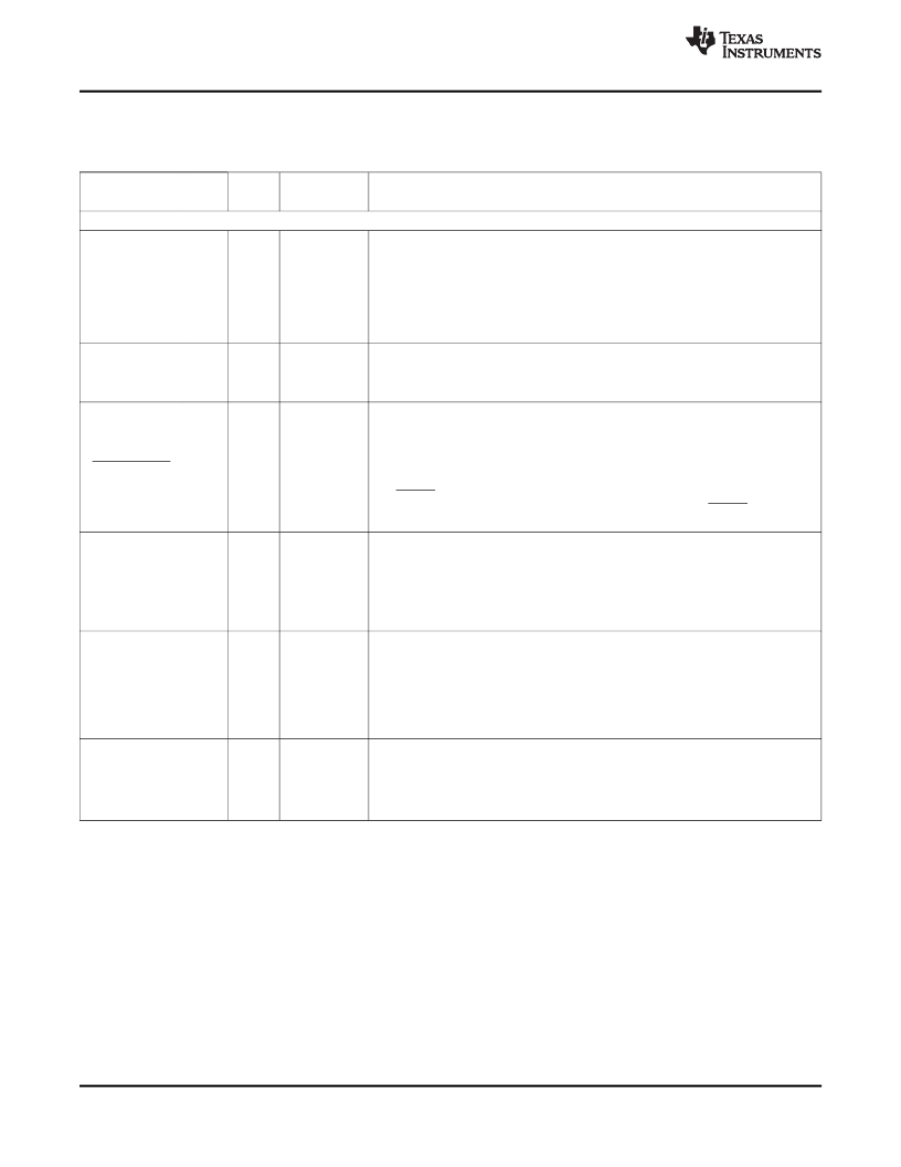
�2.5.14� Regulators� and� Power� Management� Terminal� Functions�
�Table� 2-19.� Regulators� and� Power� Management� Terminal� Functions�
��SIGNAL�
�NAME�
�NO.�
�TYPE� (1)�
�(2)�
�OTHER� (3)�
�(4)�
�DESCRIPTION�
�Regulators�
�DSP_LDO� output.� When� enabled,� this� output� provides� a� regulated� 1.3� V� or� 1.05� V�
�output� and� up� to� 250� mA� of� current� (see� the� I� SD� parameter� in� Section� 4.3� ,� Electrical�
�Characteristics� Over� Recommended� Ranges� of� Supply� Voltage� and� Operating�
�DSP_LDOO�
�E10�
�S�
�Temperature).� The� DSP_LDO� is� intended� to� supply� current� to� the� digital� core� circuits�
�only� (CV� DD� )� and� not� external� devices.� For� proper� device� operation,� the� external�
�decoupling� capacitor� of� this� pin� should� be� 5μF� ~� 10μF.� For� more� detailed�
�information,� see� Section� 5.3.4� ,� Power-Supply� Decoupling� .�
�When� disabled,� this� pin� is� in� the� high-impedance� (Hi-Z)� state.�
�LDOI�
�F14,�
�F13,�
�B12�
�S�
�LDO� inputs.� For� proper� device� operation,� LDOI� must� always� be� powered.� The� LDOI�
�pins� must� be� connected� to� the� same� power� supply� source� with� a� voltage� range� of�
�1.8� V� to� 3.6� V.� These� pins� supply� power� to� the� internal� LDOs,� the� bandgap�
�reference� generator� circuits,� and� serve� as� the� I/O� supply� for� some� input� pins.�
�DSP_LDO� enable� input.� This� signal� is� not� intended� to� be� dynamically� switched.�
�0� =� DSP_LDO� is� enabled.� The� internal� POR� monitors� the� DSP_LDOO� pin� voltage�
�and� generates� the� internal� POWERGOOD� signal.�
�DSP_LDO_EN�
�D12�
�I�
�–�
�LDOI�
�1� =� DSP_LDO� is� disabled.� The� internal� POR� voltage� monitoring� is� also� disabled.�
�The� interna� l� POWERGOOD� signal� is� forced� high� and� the� external� reset� signal� on�
�the� RESET� pin� (D6)� is� the� only� source� of� the� device� reset.� Note,� the� device's�
�internal� reset� signal� is� generated� as� the� logical� AND� of� the� RESET� pin� and� the�
�internal� POWERGOOD� signal.�
�USB_LDO� output.� This� output� provides� a� regulated� 1.3� V� output� and� up� to� 25� mA� of�
�current� (see� the� I� SD� parameter� in� Section� 4.3� ,� Electrical� Characteristics� Over�
�Recommended� Ranges� of� Supply� Voltage� and� Operating� Temperature).� For� proper�
�USB_LDOO�
�F12�
�S�
�device� operation,� this� pin� must� be� connected� to� a� 1� μ� F� ~� 2� μ� F� decoupling� capacitor�
�to� V� SS� .� For� more� detailed� information,� see� Section� 5.3.4� ,� Power-Supply� Decoupling� .�
�This� LDO� is� intended� to� supply� power� to� the� USB_� V� DD1P3� ,� USB_V� DDA1P3� pins� and�
�not� external� devices.�
�ANA_LDO� output.� This� output� provides� a� regulated� 1.3� V� output� and� up� to� 4� mA� of�
�current� (see� the� I� SD� parameter� in� Section� 4.3� ,� Electrical� Characteristics� Over�
�Recommended� Ranges� of� Supply� Voltage� and� Operating� Temperature� ).�
�ANA_LDOO�
�A12�
�S�
�For� proper� device� operation,� this� pin� must� be� connected� to� an� ~� 1.0� μ� F� decoupling�
�capacitor� to� V� SS� .� For� more� detailed� information,� see� Section� 5.3.4� ,� Power-Supply�
�Decoupling� .� This� LDO� is� intended� to� supply� power� to� the� V� DDA_ANA� and� V� DDA_PLL�
�pins� and� not� external� devices.�
�Bandgap� reference� filter� signal.� For� proper� device� operation,� this� pin� needs� to� be�
�bypassed� with� a� 0.1� μ� F� capacitor� to� analog� ground� (V� SSA_ANA� ).�
�BG_CAP�
�B13�
�A,� I/O�
�This� external� capacitor� provides� filtering� for� stable� reference� voltages� &� currents�
�generated� by� the� bandgap� circuit.� The� bandgap� produces� the� references� for� use� by�
�the� System� PLL,� SAR,� and� POR� circuits.�
�(1)�
�(2)�
�(3)�
�(4)�
�I� =� Input,� O� =� Output,� Z� =� High� impedance,� S� =� Supply� voltage,� GND� =� Ground,� A� =� Analog� signal,� BH� =� Bus� Holder�
�Input� pins� of� type� I,� I/O,� and� I/O/Z� are� required� to� be� driven� at� all� times.� To� achieve� the� lowest� power,� these� pins� must� not� be� allowed� to�
�float.� When� they� are� configured� as� input� or� high-impedance� state,� and� not� driven� to� a� known� state,� they� may� cause� an� excessive� IO-�
�supply� current.� Prevent� this� current� by� externally� terminating� it� or� enabling� IPD/IPU,� if� applicable.�
�IPD� =� Internal� pulldown,� IPU� =� Internal� pullup.� For� more� detailed� information� on� pullup/pulldown� resistors� and� situations� where� external�
�pullup/pulldown� resistors� are� required,� see� Section� 3.8.1� ,� Pullup/Pulldown� Resistors� .�
�Specifies� the� operating� I/O� supply� voltage� for� each� signal�
�42�
�Device� Overview�
��Product� Folder� Links:� TMS320C5515�
�Copyright� ?� 2010–2013,� Texas� Instruments� Incorporated�
�相关PDF资料 |
PDF描述 |
|---|---|
| RO-2405S | CONV DC/DC 1W SGL 5V OUT SIP4 |
| 37392C | INDUCTOR 3.90UH 10.0A SMD |
| IRS21834SPBF | IC DRIVER HALF-BRIDGE 14-SOIC |
| EEM24DTAD | CONN EDGECARD 48POS R/A .156 SLD |
| IR2110PBF | IC DRIVER HIGH/LOW SIDE 14DIP |
相关代理商/技术参数 |
参数描述 |
|---|---|
| TMDXBDKFP5515 | 制造商:Texas Instruments 功能描述:; Silicon Manufacturer:Texas Instruments 制造商:Texas Instruments 功能描述:TMS320C5515, FINGERPRINT SENSOR, DEV KIT |
| TMDXBEVM8148 | 制造商:Texas Instruments 功能描述:BASE EVM + POWER SUPPLY - Boxed Product (Development Kits) 制造商:Texas Instruments 功能描述:EVAL MODULE BASE & PWR SUP 制造商:Texas Instruments 功能描述:Base EVM + Power supply |
| TMDXBEVM8168B | 制造商:Texas Instruments 功能描述:NETRA DDR3 EVM SOLDERED PG1.1 SILICON - Boxed Product (Development Kits) |
| TMDXBEVM8168DDR2B | 制造商:Texas Instruments 功能描述:NETRA DDR2 EVM BETA - Bulk |
| TMDXCNCD28027 | 功能描述:开发板和工具包 - 其他处理器 Control Card RoHS:否 制造商:Freescale Semiconductor 产品:Development Systems 工具用于评估:P3041 核心:e500mc 接口类型:I2C, SPI, USB 工作电源电压: |
发布紧急采购,3分钟左右您将得到回复。