- 您现在的位置:买卖IC网 > PDF目录297613 > TMS320F241PGS (TEXAS INSTRUMENTS INC) 0-BIT, 5 MHz, OTHER DSP, PQFP64 PDF资料下载
参数资料
| 型号: | TMS320F241PGS |
| 厂商: | TEXAS INSTRUMENTS INC |
| 元件分类: | 数字信号处理 |
| 英文描述: | 0-BIT, 5 MHz, OTHER DSP, PQFP64 |
| 封装: | PLASTIC, QFP-64 |
| 文件页数: | 41/122页 |
| 文件大小: | 1465K |
| 代理商: | TMS320F241PGS |
第1页第2页第3页第4页第5页第6页第7页第8页第9页第10页第11页第12页第13页第14页第15页第16页第17页第18页第19页第20页第21页第22页第23页第24页第25页第26页第27页第28页第29页第30页第31页第32页第33页第34页第35页第36页第37页第38页第39页第40页当前第41页第42页第43页第44页第45页第46页第47页第48页第49页第50页第51页第52页第53页第54页第55页第56页第57页第58页第59页第60页第61页第62页第63页第64页第65页第66页第67页第68页第69页第70页第71页第72页第73页第74页第75页第76页第77页第78页第79页第80页第81页第82页第83页第84页第85页第86页第87页第88页第89页第90页第91页第92页第93页第94页第95页第96页第97页第98页第99页第100页第101页第102页第103页第104页第105页第106页第107页第108页第109页第110页第111页第112页第113页第114页第115页第116页第117页第118页第119页第120页第121页第122页
TMS320F243, TMS320F241
DSP CONTROLLERS
SPRS064D DECEMBER 1997 REVISED FEBRUARY 2006
25
POST OFFICE BOX 1443
HOUSTON, TEXAS 772511443
software-controlled wait-state generator (continued)
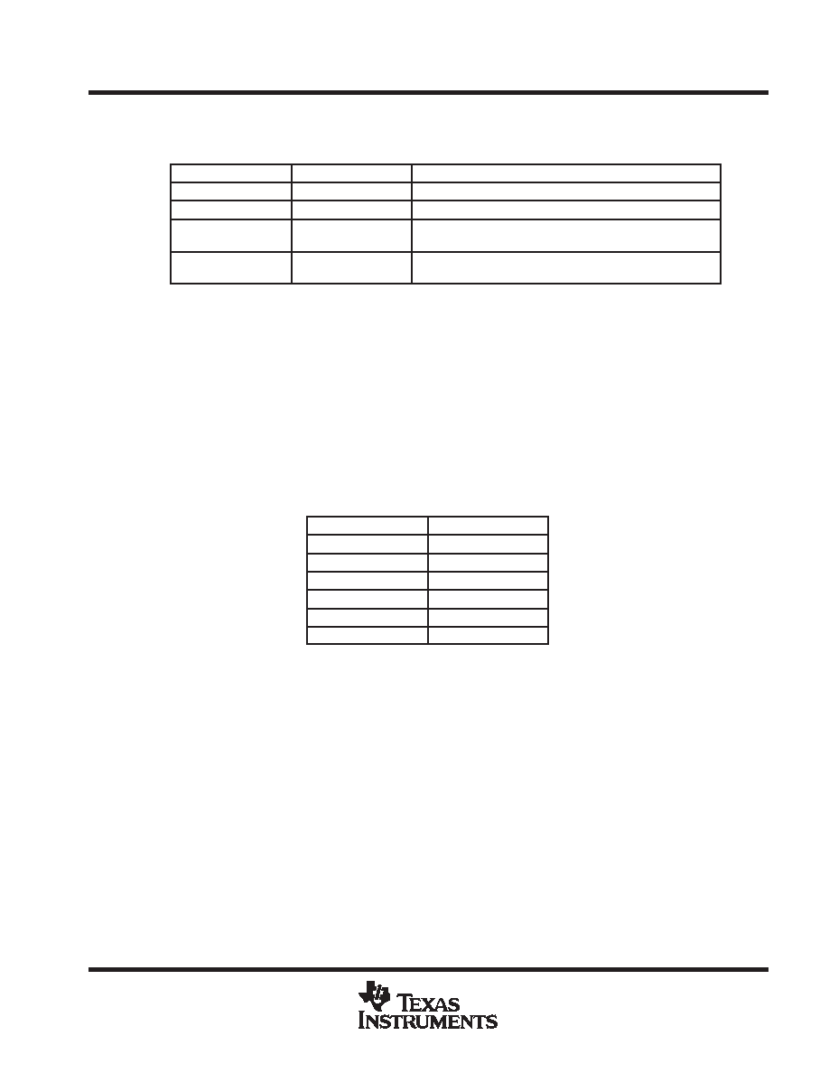
Table 6. Visibility Modes
BIT 10
BIT 9
VISIBILITY MODE
0
Bus visibility OFF (reduces power consumption and noise)
0
1
Bus visibility OFF (reduces power consumption and noise)
1
0
Data-address bus output to external address bus.
Data-data bus output to external data bus.
1
Program-address bus output to external address bus.
Program-data bus output to external data bus.
digital I/O and shared pin functions
The F243 has a total of 32 general-purpose, bidirectional, digital I/O (GPIO) pins that function as follows: six
pins are dedicated I/O pins (see Table 7) and 26 pins are shared between primary functions and I/O. The F241
has 26 I/O pins; all are shared with other functions. The digital I/O ports module provides a flexible method for
controlling both dedicated I/O and shared pin functions. All I/O and shared pin functions are controlled using
eight 16-bit registers. These registers are divided into two types:
D Output Control Registers — used to control the multiplexer selection that chooses between the primary
function of a pin or the general-purpose I/O function.
D Data and Control Registers — used to control the data and data direction of bidirectional I/O pins.
Table 7. Dedicated I/O Pins (F243 Only)
F243 PIN NUMBER
PIN NAME
20
IOPD2
21
IOPD3
23
IOPD4
25
IOPD5
27
IOPD6
29
IOPD7
description of shared I/O pins
The control structure for shared I/O pins is shown in Figure 4, where each pin has three bits that define its
operation:
D Mux control bit — this bit selects between the primary function (1) and I/O function (0) of the pin.
D I/O direction bit — if the I/O function is selected for the pin (mux control bit is set to 0), this bit determines
whether the pin is an input (0) or an output (1).
D I/O data bit — if the I/O function is selected for the pin (mux control bit is set to 0) and the direction selected
is an input, data is read from this bit; if the direction selected is an output, data is written to this bit.
The mux control bit, I/O direction bit, and I/O data bit are in the I/O control registers.
相关PDF资料 |
PDF描述 |
|---|---|
| TMS34020GBL32 | GRAPHICS PROCESSOR, CPGA145 |
| TMS34020PCML32 | GRAPHICS PROCESSOR, PQFP144 |
| TMS47C1024-30FML | 128K X 8 MASK PROM, 300 ns, PQCC32 |
| TN3041PM | 10 MHz - 300 MHz RF/MICROWAVE WIDE BAND MEDIUM POWER AMPLIFIER |
| TN5352 | 10 MHz - 300 MHz RF/MICROWAVE WIDE BAND LOW POWER AMPLIFIER |
相关代理商/技术参数 |
参数描述 |
|---|---|
| TMS320F243PGE | 功能描述:数字信号处理器和控制器 - DSP, DSC 16B 5V fixed point DSP w/ Flash RoHS:否 制造商:Microchip Technology 核心:dsPIC 数据总线宽度:16 bit 程序存储器大小:16 KB 数据 RAM 大小:2 KB 最大时钟频率:40 MHz 可编程输入/输出端数量:35 定时器数量:3 设备每秒兆指令数:50 MIPs 工作电源电压:3.3 V 最大工作温度:+ 85 C 封装 / 箱体:TQFP-44 安装风格:SMD/SMT |
| TMS320F243PGEA | 功能描述:数字信号处理器和控制器 - DSP, DSC 16B 5V fixed point DSP w/ Flash RoHS:否 制造商:Microchip Technology 核心:dsPIC 数据总线宽度:16 bit 程序存储器大小:16 KB 数据 RAM 大小:2 KB 最大时钟频率:40 MHz 可编程输入/输出端数量:35 定时器数量:3 设备每秒兆指令数:50 MIPs 工作电源电压:3.3 V 最大工作温度:+ 85 C 封装 / 箱体:TQFP-44 安装风格:SMD/SMT |
| TMS320F28015PZA | 功能描述:数字信号处理器和控制器 - DSP, DSC 32-Bit DSC w/ 32KB Flash RoHS:否 制造商:Microchip Technology 核心:dsPIC 数据总线宽度:16 bit 程序存储器大小:16 KB 数据 RAM 大小:2 KB 最大时钟频率:40 MHz 可编程输入/输出端数量:35 定时器数量:3 设备每秒兆指令数:50 MIPs 工作电源电压:3.3 V 最大工作温度:+ 85 C 封装 / 箱体:TQFP-44 安装风格:SMD/SMT |
| TMS320F28015PZA | 制造商:Texas Instruments 功能描述:IC DSP 32-BIT CMOS QFP 100PIN PLAS |
| TMS320F28015PZQ | 功能描述:数字信号处理器和控制器 - DSP, DSC 32-Bit DSC w/ 32KB Flash RoHS:否 制造商:Microchip Technology 核心:dsPIC 数据总线宽度:16 bit 程序存储器大小:16 KB 数据 RAM 大小:2 KB 最大时钟频率:40 MHz 可编程输入/输出端数量:35 定时器数量:3 设备每秒兆指令数:50 MIPs 工作电源电压:3.3 V 最大工作温度:+ 85 C 封装 / 箱体:TQFP-44 安装风格:SMD/SMT |
发布紧急采购,3分钟左右您将得到回复。