- 您现在的位置:买卖IC网 > PDF目录297613 > TMS320F241PGS (TEXAS INSTRUMENTS INC) 0-BIT, 5 MHz, OTHER DSP, PQFP64 PDF资料下载
参数资料
| 型号: | TMS320F241PGS |
| 厂商: | TEXAS INSTRUMENTS INC |
| 元件分类: | 数字信号处理 |
| 英文描述: | 0-BIT, 5 MHz, OTHER DSP, PQFP64 |
| 封装: | PLASTIC, QFP-64 |
| 文件页数: | 60/122页 |
| 文件大小: | 1465K |
| 代理商: | TMS320F241PGS |
第1页第2页第3页第4页第5页第6页第7页第8页第9页第10页第11页第12页第13页第14页第15页第16页第17页第18页第19页第20页第21页第22页第23页第24页第25页第26页第27页第28页第29页第30页第31页第32页第33页第34页第35页第36页第37页第38页第39页第40页第41页第42页第43页第44页第45页第46页第47页第48页第49页第50页第51页第52页第53页第54页第55页第56页第57页第58页第59页当前第60页第61页第62页第63页第64页第65页第66页第67页第68页第69页第70页第71页第72页第73页第74页第75页第76页第77页第78页第79页第80页第81页第82页第83页第84页第85页第86页第87页第88页第89页第90页第91页第92页第93页第94页第95页第96页第97页第98页第99页第100页第101页第102页第103页第104页第105页第106页第107页第108页第109页第110页第111页第112页第113页第114页第115页第116页第117页第118页第119页第120页第121页第122页
TMS320F243, TMS320F241
DSP CONTROLLERS
SPRS064D DECEMBER 1997 REVISED FEBRUARY 2006
42
POST OFFICE BOX 1443
HOUSTON, TEXAS 772511443
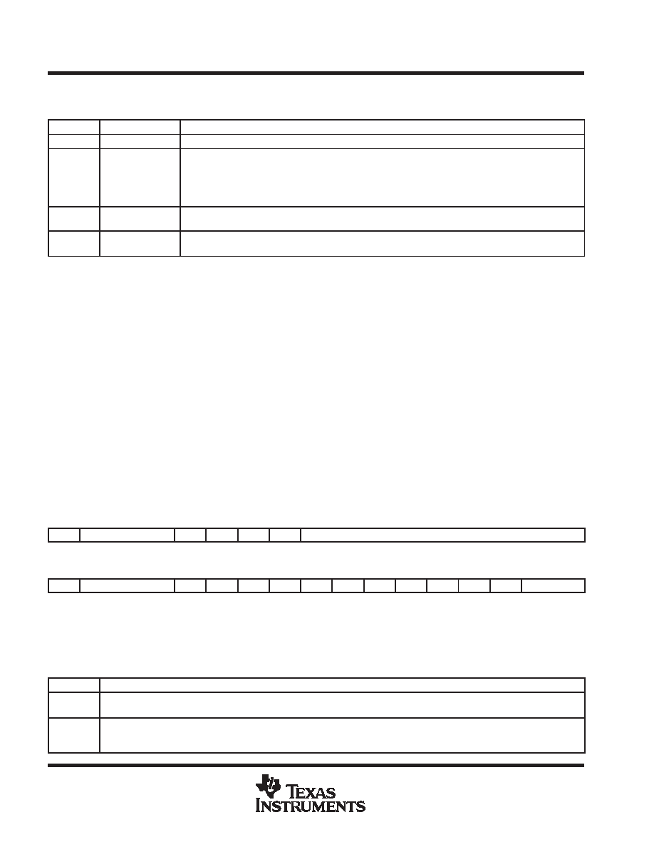
24x legend for the internal hardware (continued)
Table 13. Legend for the 24x Internal Hardware (Continued)
SYMBOL
NAME
DESCRIPTION
PREG
Product Register
32-bit register holds results of 16
× 16 multiply
PSCALE
Product-Scaling
Shifter
0-, 1-, or 4-bit left shift, or 6-bit right shift of multiplier product. The left-shift options are used to manage the
additional sign bits resulting from the 2s-complement multiply. The right-shift option is used to scale down
the number to manage overflow of product accumulation in the CALU. PSCALE resides in the path from the
32-bit product shifter and from either the CALU or the data-write data bus (DWEB), and requires no cycle
overhead.
STACK
Stack
STACK is a block of memory used for storing return addresses for subroutines and interrupt-service
routines, or for storing data. The C24x stack is 16-bit wide and eight-level deep.
TREG
Temporary
Register
16-bit register holds one of the operands for the multiply operations. TREG holds the dynamic shift count
for the LACT, ADDT, and SUBT instructions. TREG holds the dynamic bit position for the BITT instruction.
F243/F241 DSP core CPU
The TMS320x24x devices use an advanced Harvard-type architecture that maximizes processing power by
maintaining two separate memory bus structures — program and data — for full-speed execution. This multiple
bus structure allows data and instructions to be read simultaneously. Instructions support data transfers
between program memory and data memory. This architecture permits coefficients that are stored in program
memory to be read in RAM, thereby eliminating the need for a separate coefficient ROM. This, coupled with a
four-deep pipeline, allows the F243/F241 devices to execute most instructions in a single cycle.
status and control registers
Two status registers, ST0 and ST1, contain the status of various conditions and modes. These registers can
be stored into data memory and loaded from data memory, thus allowing the status of the machine to be saved
and restored for subroutines.
The load status register (LST) instruction is used to write to ST0 and ST1. The store status register (SST)
instruction is used to read from ST0 and ST1 — except for the INTM bit, which is not affected by the LST
instruction. The individual bits of these registers can be set or cleared when using the SETC and CLRC
instructions. Figure 9 shows the organization of status registers ST0 and ST1, indicating all status bits contained
in each. Several bits in the status registers are reserved and are read as logic 1s. Table 14 lists status register
field definitions.
15
13
12
11
10
9
8
0
ST0
ARP
OV
OVM
1
INTM
DP
15
13
12
11
10
9
8
7
6
5
4
3
2
1
0
ST1
ARB
CNF
TC
SXM
C
1
XF
1
PM
Figure 9. Status and Control Register Organization
Table 14. Status Register Field Definitions
FIELD
FUNCTION
ARB
Auxiliary register pointer buffer. When the ARP is loaded into ST0, the old ARP value is copied to the ARB except during an LST
instruction. When the ARB is loaded by way of an LST #1 instruction, the same value is also copied to the ARP.
ARP
Auxiliary register (AR) pointer. ARP selects the AR to be used in indirect addressing. When the ARP is loaded, the old ARP value
is copied to the ARB register. ARP can be modified by memory-reference instructions when using indirect addressing, and by the
LARP, MAR, and LST instructions. The ARP is also loaded with the same value as ARB when an LST #1 instruction is executed.
相关PDF资料 |
PDF描述 |
|---|---|
| TMS34020GBL32 | GRAPHICS PROCESSOR, CPGA145 |
| TMS34020PCML32 | GRAPHICS PROCESSOR, PQFP144 |
| TMS47C1024-30FML | 128K X 8 MASK PROM, 300 ns, PQCC32 |
| TN3041PM | 10 MHz - 300 MHz RF/MICROWAVE WIDE BAND MEDIUM POWER AMPLIFIER |
| TN5352 | 10 MHz - 300 MHz RF/MICROWAVE WIDE BAND LOW POWER AMPLIFIER |
相关代理商/技术参数 |
参数描述 |
|---|---|
| TMS320F243PGE | 功能描述:数字信号处理器和控制器 - DSP, DSC 16B 5V fixed point DSP w/ Flash RoHS:否 制造商:Microchip Technology 核心:dsPIC 数据总线宽度:16 bit 程序存储器大小:16 KB 数据 RAM 大小:2 KB 最大时钟频率:40 MHz 可编程输入/输出端数量:35 定时器数量:3 设备每秒兆指令数:50 MIPs 工作电源电压:3.3 V 最大工作温度:+ 85 C 封装 / 箱体:TQFP-44 安装风格:SMD/SMT |
| TMS320F243PGEA | 功能描述:数字信号处理器和控制器 - DSP, DSC 16B 5V fixed point DSP w/ Flash RoHS:否 制造商:Microchip Technology 核心:dsPIC 数据总线宽度:16 bit 程序存储器大小:16 KB 数据 RAM 大小:2 KB 最大时钟频率:40 MHz 可编程输入/输出端数量:35 定时器数量:3 设备每秒兆指令数:50 MIPs 工作电源电压:3.3 V 最大工作温度:+ 85 C 封装 / 箱体:TQFP-44 安装风格:SMD/SMT |
| TMS320F28015PZA | 功能描述:数字信号处理器和控制器 - DSP, DSC 32-Bit DSC w/ 32KB Flash RoHS:否 制造商:Microchip Technology 核心:dsPIC 数据总线宽度:16 bit 程序存储器大小:16 KB 数据 RAM 大小:2 KB 最大时钟频率:40 MHz 可编程输入/输出端数量:35 定时器数量:3 设备每秒兆指令数:50 MIPs 工作电源电压:3.3 V 最大工作温度:+ 85 C 封装 / 箱体:TQFP-44 安装风格:SMD/SMT |
| TMS320F28015PZA | 制造商:Texas Instruments 功能描述:IC DSP 32-BIT CMOS QFP 100PIN PLAS |
| TMS320F28015PZQ | 功能描述:数字信号处理器和控制器 - DSP, DSC 32-Bit DSC w/ 32KB Flash RoHS:否 制造商:Microchip Technology 核心:dsPIC 数据总线宽度:16 bit 程序存储器大小:16 KB 数据 RAM 大小:2 KB 最大时钟频率:40 MHz 可编程输入/输出端数量:35 定时器数量:3 设备每秒兆指令数:50 MIPs 工作电源电压:3.3 V 最大工作温度:+ 85 C 封装 / 箱体:TQFP-44 安装风格:SMD/SMT |
发布紧急采购,3分钟左右您将得到回复。