参数资料
| 型号: | XRT75R12DIB-L |
| 厂商: | Exar Corporation |
| 文件页数: | 120/133页 |
| 文件大小: | 0K |
| 描述: | IC LIU E3/DS3/STS-1 12CH 420TBGA |
| 标准包装: | 40 |
| 类型: | 线路接口装置(LIU) |
| 驱动器/接收器数: | 12/12 |
| 规程: | DS3,E3,STS-1 |
| 电源电压: | 3.135 V ~ 3.465 V |
| 安装类型: | 表面贴装 |
| 封装/外壳: | 420-LBGA 裸露焊盘 |
| 供应商设备封装: | 420-TBGA(35x35) |
| 包装: | 托盘 |
第1页第2页第3页第4页第5页第6页第7页第8页第9页第10页第11页第12页第13页第14页第15页第16页第17页第18页第19页第20页第21页第22页第23页第24页第25页第26页第27页第28页第29页第30页第31页第32页第33页第34页第35页第36页第37页第38页第39页第40页第41页第42页第43页第44页第45页第46页第47页第48页第49页第50页第51页第52页第53页第54页第55页第56页第57页第58页第59页第60页第61页第62页第63页第64页第65页第66页第67页第68页第69页第70页第71页第72页第73页第74页第75页第76页第77页第78页第79页第80页第81页第82页第83页第84页第85页第86页第87页第88页第89页第90页第91页第92页第93页第94页第95页第96页第97页第98页第99页第100页第101页第102页第103页第104页第105页第106页第107页第108页第109页第110页第111页第112页第113页第114页第115页第116页第117页第118页第119页当前第120页第121页第122页第123页第124页第125页第126页第127页第128页第129页第130页第131页第132页第133页
XRT75R12D
83
REV. 1.0.3
TWELVE CHANNEL E3/DS3/STS-1 LINE INTERFACE UNIT WITH SONET DESYNCHRONIZER
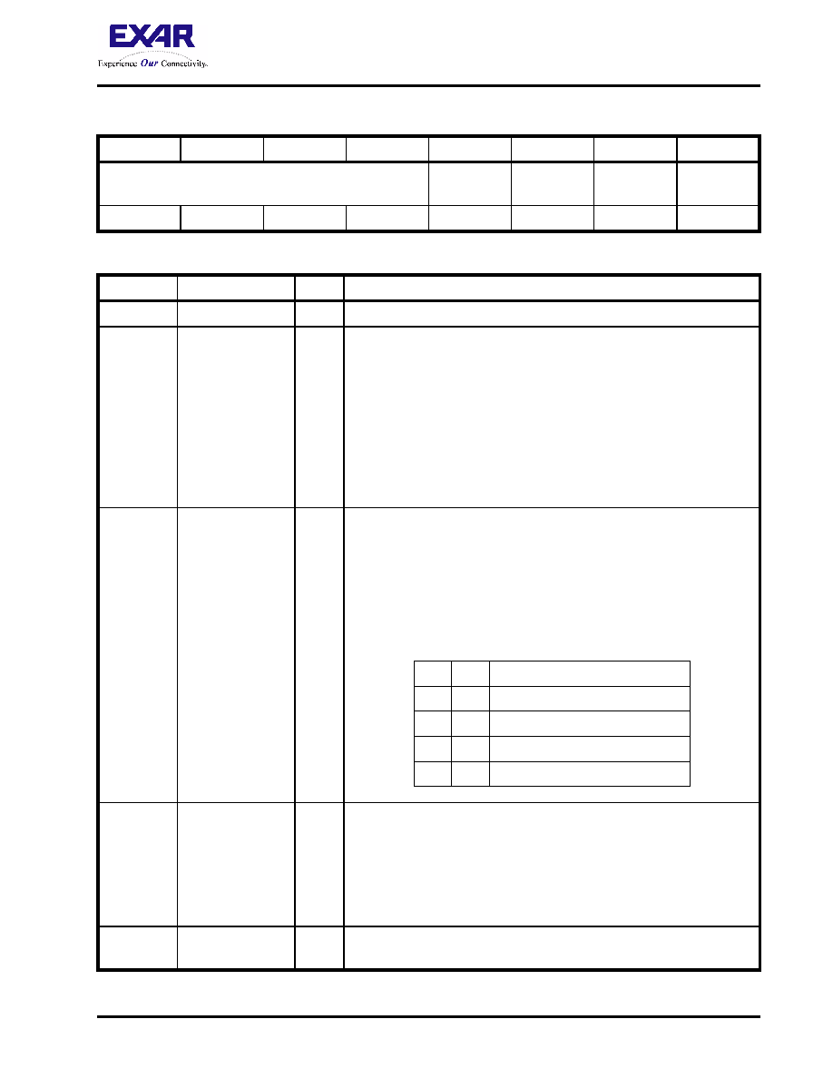
TABLE 36: XRT75R12D REGISTER MAP SHOWING JITTER ATTENUATOR CONTROL REGISTERS (JA_N) (N = [0:11])
BIT 7
BIT 6
BIT 5
BIT 4
BIT 3
BIT 2
BIT 1
BIT 0
Reserved
JA RESET
Ch_n
JA1 Ch_n
JA in Tx Path
Ch_n
JA0 Ch_n
R/W
JITTER ATTENUATOR CONTROL REGISTER - CHANNEL N ADDRESS LOCATION = 0XM7 (M = 0-5 & 8-D)
BIT NUMBER
NAME
TYPE
DESCRIPTION
7 - 4
Reserved
3
JA RESET Ch_n
R/W
Jitter Attenuator RESET - Channel_n:
Writing a "0 to 1" transition within this bit-field will configure the Jitter Attenu-
ator (within Channel_n) to execute a RESET operation.
Whenever the user executes a RESET operation, then following will occur.
The READ and WRITE pointers (within the Jitter Attenuator FIFO) will be
reset to their default values.
The contents of the Jitter Attenuator FIFO will be flushed.
NOTE: The user must follow up any "0 to 1" transition with the appropriate
write operate to set this bit-field back to "0", in order to resume
normal operation with the Jitter Attenuator.
2
JA1 Ch_n
R/W
Jitter Attenuator Configuration Select Input - Bit 1:
This READ/WRITE bit-field, along with Bit 0 (JA0 Ch_n) is used to do any of
the following.
To enable or disable the Jitter Attenuator corresponding to Channel_n.
To select the FIFO Depth for the Jitter Attenuator within Channel_n.
The relationship between the settings of these two bit-fields and the Enable/
Disable States, and FIFO Depths is presented below.
1
JA in Tx Path Ch_n
R/W
Jitter Attenuator in Transmit/Receive Path Select Bit:
This input pin is used to configure the Jitter Attenuator (within Channel_n) to
operate in either the Transmit or Receive path, as described below.
0 - Configures the Jitter Attenuator (within Channel_n) to operate in the
Receive Path.
1 - Configures the Jitter Attenuator (within Channel_n) to operate in the
Transmit Path.
0
JA0 Ch_n
R/W
Jitter Attenuator Configuration Select Input - Bit 0:
See the description for Bit 2 (JA1 Ch_n).
JA0
JA1
Jitter Attenuator Mode
1
Disabled
1
0
SONET/SDH De-Sync Mode
0
1
FIFO Depth = 32 bits
0
FIFO Depth = 16 bits
相关PDF资料 |
PDF描述 |
|---|---|
| XRT75R12IB-L | IC LIU E3/DS3/STS-1 12CH 420TBGA |
| XRT75VL00DIV | IC LIU E3/DS3/STS-1 1CH 52TQFP |
| XRT75VL00IV-F | IC LIU E3/DS3/STS-1 1CH 52TQFP |
| XRT79L71IB-F | IC LIU/FRAMER DS3/E3 1CH 208BGA |
| XRT81L27IV-F | IC LIU EI 7CH 3.3V 128TQFP |
相关代理商/技术参数 |
参数描述 |
|---|---|
| XRT75R12ES | 功能描述:时钟合成器/抖动清除器 12CH T3/E3/STS1LIUJA 3.3V W/REDUNDANCY RoHS:否 制造商:Skyworks Solutions, Inc. 输出端数量: 输出电平: 最大输出频率: 输入电平: 最大输入频率:6.1 GHz 电源电压-最大:3.3 V 电源电压-最小:2.7 V 封装 / 箱体:TSSOP-28 封装:Reel |
| XRT75R12IB | 功能描述:外围驱动器与原件 - PCI 12CH E3/DS3/STS W/JITTER R3 TECH RoHS:否 制造商:PLX Technology 工作电源电压: 最大工作温度: 安装风格:SMD/SMT 封装 / 箱体:FCBGA-1156 封装:Tray |
| XRT75R12IB-F | 功能描述:外围驱动器与原件 - PCI 12 Channel 3.3V-5V temp -45 to 85C RoHS:否 制造商:PLX Technology 工作电源电压: 最大工作温度: 安装风格:SMD/SMT 封装 / 箱体:FCBGA-1156 封装:Tray |
| XRT75R12IB-L | 功能描述:LIN 收发器 Attenuator RoHS:否 制造商:NXP Semiconductors 工作电源电压: 电源电流: 最大工作温度: 封装 / 箱体:SO-8 |
| XRT75VL00 | 制造商:EXAR 制造商全称:EXAR 功能描述:E3/DS3/STS-1 LINE INTERFACE UNIT WITH JITTER ATTENUATOR |
发布紧急采购,3分钟左右您将得到回复。