参数资料
| 型号: | XRT75R12DIB-L |
| 厂商: | Exar Corporation |
| 文件页数: | 15/133页 |
| 文件大小: | 0K |
| 描述: | IC LIU E3/DS3/STS-1 12CH 420TBGA |
| 标准包装: | 40 |
| 类型: | 线路接口装置(LIU) |
| 驱动器/接收器数: | 12/12 |
| 规程: | DS3,E3,STS-1 |
| 电源电压: | 3.135 V ~ 3.465 V |
| 安装类型: | 表面贴装 |
| 封装/外壳: | 420-LBGA 裸露焊盘 |
| 供应商设备封装: | 420-TBGA(35x35) |
| 包装: | 托盘 |
第1页第2页第3页第4页第5页第6页第7页第8页第9页第10页第11页第12页第13页第14页当前第15页第16页第17页第18页第19页第20页第21页第22页第23页第24页第25页第26页第27页第28页第29页第30页第31页第32页第33页第34页第35页第36页第37页第38页第39页第40页第41页第42页第43页第44页第45页第46页第47页第48页第49页第50页第51页第52页第53页第54页第55页第56页第57页第58页第59页第60页第61页第62页第63页第64页第65页第66页第67页第68页第69页第70页第71页第72页第73页第74页第75页第76页第77页第78页第79页第80页第81页第82页第83页第84页第85页第86页第87页第88页第89页第90页第91页第92页第93页第94页第95页第96页第97页第98页第99页第100页第101页第102页第103页第104页第105页第106页第107页第108页第109页第110页第111页第112页第113页第114页第115页第116页第117页第118页第119页第120页第121页第122页第123页第124页第125页第126页第127页第128页第129页第130页第131页第132页第133页
XRT75R12D
107
REV. 1.0.3
TWELVE CHANNEL E3/DS3/STS-1 LINE INTERFACE UNIT WITH SONET DESYNCHRONIZER
8.3.4
Why are we talking about Pointer Adjustments?
The overall SONET network consists of numerous "Synchronization Islands". As a consequence, whenever a
SONET signal is being transmitted from one "Synchronization Island" to another; that SONET signal will
undergo a "clock domain" change as it traverses the network. This clock domain change will result in periodic
pointer-adjustments occurring within this SONET signal. Depending upon the direction of this "clock-domain"
shift that the SONET signal experiences, there will either be periodic "incrementing" pointer-adjustment events
or periodic "decrementing" pointer-adjustment events within this SONET signal.
Regardless of whether a given SONET signal is experiencing incrementing or decrementing pointer
adjustment events, each pointer adjustment event will result in an abrupt 8-bit shift in the position of the SPE
within the STS-1 data-stream. If this STS-1 signal is transporting an "asynchronously-mapped" DS3 signal;
then this 8-bit shift in the location of the SPE (within the STS-1 signal) will result in approximately 8UIpp of jitter
within the asynchronously-mapped DS3 signal, as it is de-mapped from SONET. In “Section 8.5, A Review of
the Category I Intrinsic Jitter Requirements (per Telcordia GR-253-CORE) for DS3 applications” on
page 108 we will discuss the "Category I Intrinsic Jitter Requirements (for DS3 Applications) per Telcordia GR-
253-CORE. However, for now we will simply state that this 8UIpp of intrinsic jitter far exceeds these "intrinsic
jitter" requirements.
In summary, pointer-adjustments events are a "fact of life" within the SONET/SDH network. Further, pointer-
adjustment events, within a SONET signal that is transporting an asynchronously-mapped DS3 signal, will
impose a significant impact on the Intrinsic Jitter and Wander within that DS3 signal as it is de-mapped from
SONET.
8.4
Clock Gapping Jitter
In most applications (in which the LIU will be used in a SONET De-Sync Application) the user will typically
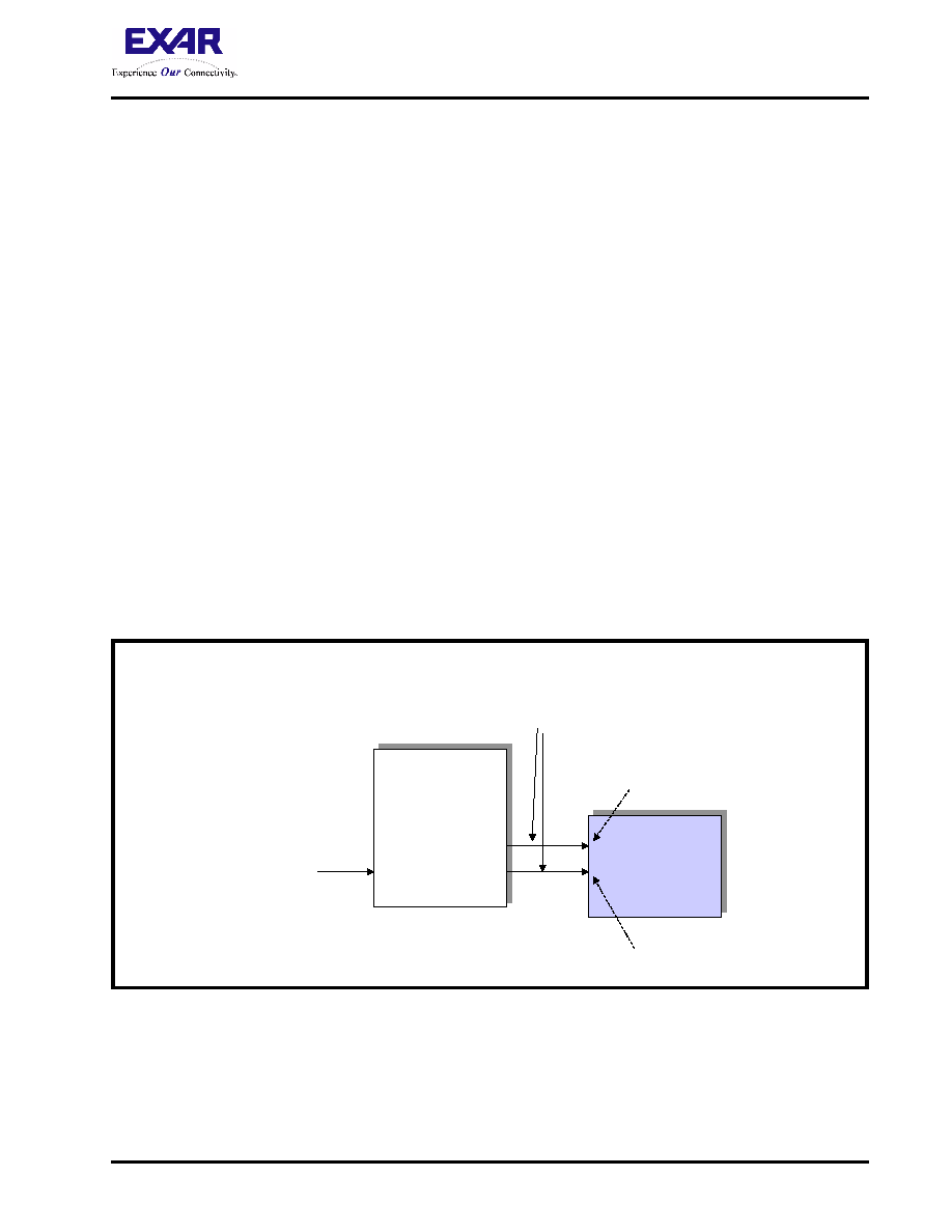
interface the LIU to a Mapper Device in the manner as presented below in Figure 54.
In this application, the Mapper IC will have the responsibility of receiving an STS-N signal (from the SONET
Network) and performing all of the following operations on this STS-N signal.
Byte-de-interleaving this incoming STS-N signal into N STS-1 signals
Terminating each of these STS-1 signals
Extracting (or de-mapping) the DS3 signal(s) from the SPEs within each of these terminated STS-1 signals.
FIGURE 54. ILLUSTRATION OF THE TYPICAL APPLICATIONS FOR THE LIU IN A SONET DE-SYNC APPLICATION
DS3 to STS-N
Mapper/
Demapper
IC
DS3 to STS-N
Mapper/
Demapper
IC
LIU
STS-N Signal
TPDATA_n input pin
TCLK_n input
De-Mapped (Gapped)
DS3 Data and Clock
相关PDF资料 |
PDF描述 |
|---|---|
| XRT75R12IB-L | IC LIU E3/DS3/STS-1 12CH 420TBGA |
| XRT75VL00DIV | IC LIU E3/DS3/STS-1 1CH 52TQFP |
| XRT75VL00IV-F | IC LIU E3/DS3/STS-1 1CH 52TQFP |
| XRT79L71IB-F | IC LIU/FRAMER DS3/E3 1CH 208BGA |
| XRT81L27IV-F | IC LIU EI 7CH 3.3V 128TQFP |
相关代理商/技术参数 |
参数描述 |
|---|---|
| XRT75R12ES | 功能描述:时钟合成器/抖动清除器 12CH T3/E3/STS1LIUJA 3.3V W/REDUNDANCY RoHS:否 制造商:Skyworks Solutions, Inc. 输出端数量: 输出电平: 最大输出频率: 输入电平: 最大输入频率:6.1 GHz 电源电压-最大:3.3 V 电源电压-最小:2.7 V 封装 / 箱体:TSSOP-28 封装:Reel |
| XRT75R12IB | 功能描述:外围驱动器与原件 - PCI 12CH E3/DS3/STS W/JITTER R3 TECH RoHS:否 制造商:PLX Technology 工作电源电压: 最大工作温度: 安装风格:SMD/SMT 封装 / 箱体:FCBGA-1156 封装:Tray |
| XRT75R12IB-F | 功能描述:外围驱动器与原件 - PCI 12 Channel 3.3V-5V temp -45 to 85C RoHS:否 制造商:PLX Technology 工作电源电压: 最大工作温度: 安装风格:SMD/SMT 封装 / 箱体:FCBGA-1156 封装:Tray |
| XRT75R12IB-L | 功能描述:LIN 收发器 Attenuator RoHS:否 制造商:NXP Semiconductors 工作电源电压: 电源电流: 最大工作温度: 封装 / 箱体:SO-8 |
| XRT75VL00 | 制造商:EXAR 制造商全称:EXAR 功能描述:E3/DS3/STS-1 LINE INTERFACE UNIT WITH JITTER ATTENUATOR |
发布紧急采购,3分钟左右您将得到回复。