- 您现在的位置:买卖IC网 > PDF目录15166 > ZL6105ALAFTK (Intersil)IC REG CTRLR BUCK PWM VM 36-QFN PDF资料下载
参数资料
| 型号: | ZL6105ALAFTK |
| 厂商: | Intersil |
| 文件页数: | 17/35页 |
| 文件大小: | 0K |
| 描述: | IC REG CTRLR BUCK PWM VM 36-QFN |
| 标准包装: | 1,000 |
| PWM 型: | 电压模式 |
| 输出数: | 1 |
| 频率 - 最大: | 1.4MHz |
| 占空比: | 95% |
| 电源电压: | 3 V ~ 14 V |
| 降压: | 是 |
| 升压: | 无 |
| 回扫: | 无 |
| 反相: | 无 |
| 倍增器: | 无 |
| 除法器: | 无 |
| Cuk: | 无 |
| 隔离: | 无 |
| 工作温度: | -40°C ~ 85°C |
| 封装/外壳: | 36-VFQFN 裸露焊盘 |
| 包装: | 带卷 (TR) |
第1页第2页第3页第4页第5页第6页第7页第8页第9页第10页第11页第12页第13页第14页第15页第16页当前第17页第18页第19页第20页第21页第22页第23页第24页第25页第26页第27页第28页第29页第30页第31页第32页第33页第34页第35页
�� �
�
�ZL6105�
�(� I� )�
�I� Lrms� =� I� OUT� +�
�by� increasing� the� switching� frequency� at� the� expense� of�
�efficiency.� Cost� can� be� minimized� by� using� through-hole�
�inductors� and� capacitors;� however� these� components� are�
�physically� large.�
�I� Lrms� is� given� by� Equation� 9.�
�2� opp�
�12�
�2�
�(EQ.� 9)�
�To� start� the� design,� select� a� switching� frequency� based� on� Table�
�13.� This� frequency� is� a� starting� point� and� may� be� adjusted� as� the�
�design� progresses.�
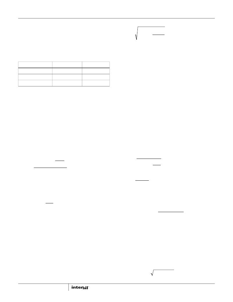
�TABLE� 13.� CIRCUIT� DESIGN� CONSIDERATIONS�
�where� I� OUT� is� the� maximum� output� current.� Next,� calculate� the�
�core� loss� of� the� selected� inductor.� Since� this� calculation� is�
�specific� to� each� inductor� and� manufacturer,� refer� to� the� chosen�
�inductor� datasheet.� Add� the� core� loss� and� the� ESR� loss� and�
�compare� the� total� loss� to� the� maximum� power� dissipation�
�FREQUENCY� RANGE�
�200kHz� to� 400kHz�
�400kHz� to� 800kHz�
�EFFICIENCY�
�Highest�
�Moderate�
�CIRCUIT� SIZE�
�Larger�
�Smaller�
�recommendation� in� the� inductor� datasheet.�
�OUTPUT� CAPACITOR� SELECTION�
�Several� trade-offs� must� also� be� considered� when� selecting� an�
�800kHz� to� 1.4MHz� Lower� Smallest�
�INDUCTOR� SELECTION�
�The� output� inductor� selection� process� must� include� several�
�trade-offs.� A� high� inductance� value� will� result� in� a� low� ripple�
�current� (I� O(P-P)� ),� which� will� reduce� output� capacitance� and�
�produce� a� low� output� ripple� voltage,� but� may� also� compromise�
�output� transient� load� performance.� Therefore,� a� balance� must� be�
�struck� between� output� ripple� and� optimal� load� transient�
�performance.� A� good� starting� point� is� to� select� the� output�
�inductor� ripple� equal� to� the� expected� load� transient� step�
�output� capacitor.� Low� ESR� values� are� needed� to� have� a� small�
�output� deviation� during� transient� load� steps� (V� OSAG� )� and� low�
�output� voltage� ripple� (V� ORIP� ).� However,� capacitors� with� low� ESR,�
�such� as� semi-stable� (X5R� and� X7R)� dielectric� ceramic� capacitors,�
�also� have� relatively� low� capacitance� values.� Many� designs� can�
�use� a� combination� of� high� capacitance� devices� and� low� ESR�
�devices� in� parallel.�
�For� high� ripple� currents,� a� low� capacitance� value� can� cause� a�
�significant� amount� of� output� voltage� ripple.� Likewise,� in� high�
�transient� load� steps,� a� relatively� large� amount� of� capacitance� is�
�needed� to� minimize� the� output� voltage� deviation� while� the�
�magnitude� (I� OSTEP� )� as� shown� in� Equation� 5:�
�I� opp� =� I� ostep�
�(EQ.� 5)�
�inductor� current� ramps� up� or� down� to� the� new� steady� state�
�output� current� value.�
�As� a� starting� point,� apportion� one-half� of� the� output� ripple�
�voltage� to� the� capacitor� ESR� and� the� other� half� to� capacitance,� as�
�Now� the� output� inductance� can� be� calculated� using� Equation� 6:�
�shown� in� the� Equations� 10� and� 11:�
�V� OUT� � ?� ?� 1� ?� OUT�
�?� ?�
�L� OUT�
�=�
�?� V�
�?� V� INM�
�fsw� � I� opp�
�?�
�?�
�(EQ.� 6)�
�C� OUT� =�
�I� opp�
�8� � f� sw� �
�V� orip�
�2�
�(EQ.� 10)�
�ESR� =�
�V� orip�
�I� Lpk� =� I� OUT� +�
�I� opp�
�V� orip� =� I� opp� � ESR� +�
�I� opp�
�P� LDCR� =� DCR� � I� Lrms�
�(EQ.� 8)�
�I� CINrms� =� I� OUT� � D� � (� 1� ?� D� )�
�where� V� INM� is� the� maximum� input� voltage.�
�The� average� inductor� current� is� equal� to� the� maximum� output�
�current.� The� peak� inductor� current� (I� Lpk� )� is� calculated� using�
�Equation� 7:�
�(EQ.� 7)�
�2�
�where� I� OUT� is� the� maximum� output� current.�
�Select� an� inductor� rated� for� the� average� DC� current� with� a� peak�
�current� rating� above� the� peak� current� computed� in� Equation� 7.�
�In� overcurrent� or� short-circuit� conditions,� the� inductor� may� have�
�currents� greater� than� 2x� the� normal� maximum� rated� output�
�current.� It� is� desirable� to� use� an� inductor� that� still� provides� some�
�inductance� to� protect� the� load� and� the� MOSFETs� from� damaging�
�currents� in� this� situation.�
�Once� an� inductor� is� selected,� the� DCR� and� core� losses� in� the�
�inductor� are� calculated� as� in� Equation� 8.� Use� the� DCR� specified� in�
�the� inductor� manufacturer’s� datasheet.�
�2�
�17�
�(EQ.� 11)�
�2� � I� opp�
�Use� these� values� to� make� an� initial� capacitor� selection,� using� a�
�single� capacitor� or� several� capacitors� in� parallel.�
�After� a� capacitor� has� been� selected,� the� resulting� output� voltage�
�ripple� can� be� calculated� using� Equation� 12:�
�(EQ.� 12)�
�8� � f� sw� � C� OUT�
�Because� each� part� of� this� equation� was� made� to� be� less� than� or�
�equal� to� half� of� the� allowed� output� ripple� voltage,� the� V� ORIP�
�should� be� less� than� the� desired� maximum� output� ripple.�
�INPUT� CAPACITOR�
�It� is� highly� recommended� that� dedicated� input� capacitors� be�
�used� in� any� point-of-load� design,� even� when� the� supply� is�
�powered� from� a� heavily� filtered� 5V� or� 12V� “bulk”� supply� from� an�
�off-line� power� supply.� This� is� because� of� the� high� RMS� ripple�
�current� that� is� drawn� by� the� buck� converter� topology.� This� ripple�
�(I� CINrms� )� can� be� determined� from� Equation� 13:�
�(EQ.� 13)�
�FN6906.5�
�December� 19,� 2013�
�相关PDF资料 |
PDF描述 |
|---|---|
| RBM18DREI | CONN EDGECARD 36POS .156 EYELET |
| B43086F2476M | 47UF 250V 16X20 SINGLE END |
| ISL6307CRZ-T | IC REG CTRLR BUCK PWM VM 48-QFN |
| ISL6401CB-T | IC REG CTRLR PWM CM 14-SOIC |
| GCM18DREF | CONN EDGECARD 36POS .156 EYELET |
相关代理商/技术参数 |
参数描述 |
|---|---|
| ZL6105ALAFTKR5546 | 功能描述:DC/DC 开关控制器 RoHS:否 制造商:Texas Instruments 输入电压:6 V to 100 V 开关频率: 输出电压:1.215 V to 80 V 输出电流:3.5 A 输出端数量:1 最大工作温度:+ 125 C 安装风格: 封装 / 箱体:CPAK |
| ZL6105ALAFTKR5549 | 制造商:Intersil Corporation 功能描述:ADAPTIVE DIGITAL DC-DC CONTROLLER W/ DRIVERS & I-SHARING FE0 - Tape and Reel |
| ZL6105ALAFTKR5553 | 制造商:Intersil Corporation 功能描述:ADAPTIVE DIGITAL DC-DC CONTROLLER W/ DRIVERS & I-SHARING MOD - Tape and Reel |
| ZL6105ALAFTKR5554 | 制造商:Intersil Corporation 功能描述:ADAPTIVE DIGITAL DC-DC CONTROLLER W/ DRIVERS & I-SHARING MOD - Tape and Reel |
| ZL6105ALAFTR5546 | 功能描述:IC REG CTRLR BUCK PWM VM 36-QFN RoHS:是 类别:集成电路 (IC) >> PMIC - 稳压器 - DC DC 切换控制器 系列:- 产品培训模块:Lead (SnPb) Finish for COTS Obsolescence Mitigation Program 标准包装:2,500 系列:- PWM 型:电流模式 输出数:1 频率 - 最大:275kHz 占空比:50% 电源电压:18 V ~ 110 V 降压:无 升压:无 回扫:无 反相:无 倍增器:无 除法器:无 Cuk:无 隔离:是 工作温度:-40°C ~ 85°C 封装/外壳:8-SOIC(0.154",3.90mm 宽) 包装:带卷 (TR) |
发布紧急采购,3分钟左右您将得到回复。