- 您现在的位置:买卖IC网 > PDF目录15166 > ZL6105ALAFTK (Intersil)IC REG CTRLR BUCK PWM VM 36-QFN PDF资料下载
参数资料
| 型号: | ZL6105ALAFTK |
| 厂商: | Intersil |
| 文件页数: | 18/35页 |
| 文件大小: | 0K |
| 描述: | IC REG CTRLR BUCK PWM VM 36-QFN |
| 标准包装: | 1,000 |
| PWM 型: | 电压模式 |
| 输出数: | 1 |
| 频率 - 最大: | 1.4MHz |
| 占空比: | 95% |
| 电源电压: | 3 V ~ 14 V |
| 降压: | 是 |
| 升压: | 无 |
| 回扫: | 无 |
| 反相: | 无 |
| 倍增器: | 无 |
| 除法器: | 无 |
| Cuk: | 无 |
| 隔离: | 无 |
| 工作温度: | -40°C ~ 85°C |
| 封装/外壳: | 36-VFQFN 裸露焊盘 |
| 包装: | 带卷 (TR) |
第1页第2页第3页第4页第5页第6页第7页第8页第9页第10页第11页第12页第13页第14页第15页第16页第17页当前第18页第19页第20页第21页第22页第23页第24页第25页第26页第27页第28页第29页第30页第31页第32页第33页第34页第35页
�� �
�
�ZL6105�
�Without� capacitive� filtering� near� the� power� supply� circuit,� this�
�current� would� flow� through� the� supply� bus� and� return� planes,�
�I� toprms� =� I� Lrms� � D�
�(EQ.� 19)�
�P� QH� =� 0� .� 05� � V� OUT� � I� OUT�
�R� DS� (� ON� )� =�
�(� I� )�
�t� SW� =�
�Q� g�
�coupling� noise� into� other� system� circuitry.� The� input� capacitors�
�should� be� rated� at� 1.2x� the� ripple� current� calculated� in� Equation�
�13� to� avoid� overheating� of� the� capacitors� due� to� the� high� ripple�
�current,� which� can� cause� premature� failure.� Ceramic� capacitors�
�with� X7R� or� X5R� dielectric� with� low� ESR� and� 1.1x� the� maximum�
�expected� input� voltage� are� recommended.�
�BOOTSTRAP� CAPACITOR� SELECTION�
�The� high-side� driver� boost� circuit� utilizes� an� external� Schottky� diode�
�(D� B� )� and� an� external� bootstrap� capacitor� (C� B� )� to� supply� sufficient�
�gate� drive� for� the� high-side� MOSFET� driver.� D� B� should� be� a� 20mA,�
�30V� Schottky� diode� or� equivalent� device� and� C� B� should� be� a� 1μF�
�ceramic� type� rated� for� at� least� 6.3V.�
�QL� SELECTION�
�The� bottom� MOSFET� should� be� selected� primarily� based� on� the�
�device’s� r� DS(ON)� and� secondarily� based� on� its� gate� charge.� To�
�choose� QL,� use� Equation� 14� and� allow� 2%� to� 5%� of� the� output�
�power� to� be� dissipated� in� the� r� DS(ON)� of� QL� (lower� output� voltages�
�and� higher� step-down� ratios� will� be� closer� to� 5%):�
�Calculate� a� starting� r� DS(ON)� as� shown� in� Equation� 20.� This�
�equation� uses� 5%� as� an� example:�
�(EQ.� 20)�
�P� QH�
�(EQ.� 21)�
�2�
�toprms�
�Select� a� MOSFET� and� calculate� the� resulting� gate� drive� current.�
�Verify� that� the� combined� gate� drive� current� from� QL� and� QH� does�
�not� exceed� 80mA.�
�Next,� calculate� the� switching� time� using� Equation� 22:�
�(EQ.� 22)�
�I� gdr�
�where� Q� g� is� the� gate� charge� of� the� selected� QH� and� I� gdr� is� the�
�peak� gate� drive� current� available� from� the� ZL6105.�
�P� QL� =� 0� .� 05� � V� OUT� � I� OUT�
�(EQ.� 14)�
�Although� the� ZL6105� has� a� typical� gate� drive� current� of� 3A,� use�
�the� minimum� guaranteed� current� of� 2A� for� a� conservative�
�I� botrms� =� I� Lrms� � 1� ?� D�
�R� DS� (� ON� )� =�
�P� QL�
�(� I� botrms� )� 2�
�P� swtop� =� V� INM� � t� sw� � I� OUT� � f� sw�
�P� QHtot� =� P� QH� +� P� swtop�
�I� g� =� f� SW� � Q� g�
�T� j� max� =� T� pcb� +� (� P� Q� � R� th� )�
�P� QL� =� f� sw� � Q� g� � V� INM�
�Calculate� the� RMS� current� in� QL� as� shown� in� Equation� 15:�
�(EQ.� 15)�
�Calculate� the� desired� maximum� r� DS(ON)� as� shown� in� Equation� 16:�
�(EQ.� 16)�
�Note� that� the� r� DS(ON)� given� in� the� manufacturer’s� datasheet� is�
�measured� at� +25°C.� The� actual� r� DS(ON)� in� the� end-use� application�
�will� be� much� higher.� For� example,� a� Vishay� Si7114� MOSFET� with�
�a� junction� temperature� of� +125°C� has� an� r� DS(ON)� that� is� 1.4x�
�higher� than� the� value� at� +25°C.� Select� a� candidate� MOSFET,� and�
�calculate� the� required� gate� drive� current� as� shown� in� Equation�
�17:�
�(EQ.� 17)�
�Keep� in� mind� that� the� total� allowed� gate� drive� current� for� both� QH�
�and� QL� is� 80mA.�
�MOSFETs� with� lower� r� DS(ON)� tend� to� have� higher� gate� charge�
�requirements,� which� increases� the� current� and� resulting� power�
�required� to� turn� them� on� and� off.� Since� the� MOSFET� gate� drive�
�circuits� are� integrated� in� the� ZL6105,� this� power� is� dissipated� in�
�the� ZL6105� according� to� the� Equation� 18:�
�(EQ.� 18)�
�design.� Using� the� calculated� switching� time,� calculate� the�
�switching� power� loss� in� QH� using� Equation� 23:�
�(EQ.� 23)�
�The� total� power� dissipated� by� QH� is� given� by� Equation� 24:�
�(EQ.� 24)�
�MOSFET� THERMAL� CHECK�
�Once� the� power� dissipations� for� QH� and� QL� have� been� calculated,�
�the� MOSFETs� junction� temperature� can� be� estimated.� Using� the�
�junction-to-case� thermal� resistance� (R� th� )� given� in� the� MOSFET�
�manufacturer’s� datasheet� and� the� expected� maximum� printed�
�circuit� board� temperature,� calculate� the� junction� temperature� as�
�shown� in� Equation� 25:�
�(EQ.� 25)�
�CURRENT� SENSING� COMPONENTS�
�Once� the� current� sense� method� has� been� selected� (Refer� to�
��components� are� selected� as� indicated� in� the� following.�
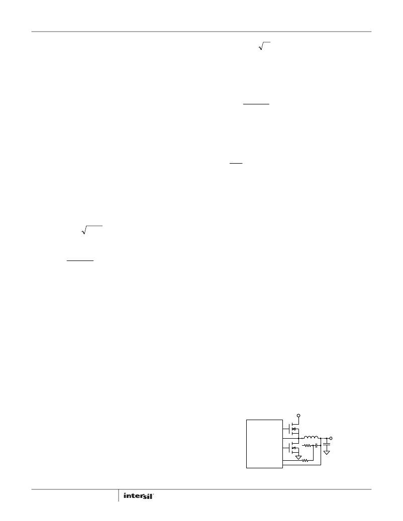
�When� using� the� inductor� DCR� sensing� method,� the� user� must�
�also� select� an� R/C� network� comprised� of� R1� and� CL� (see�
�Figure� 11).�
�QH� SELECTION�
�In� addition� to� the� r� DS(ON)� loss� and� gate� charge� loss,� QH� also� has�
�switching� loss.� The� procedure� to� select� QH� is� similar� to� the�
�procedure� for� QL.� First,� assign� 2%� to� 5%� of� the� output� power� to�
�ZL�
�GH�
�SW�
�GL�
�R1�
�CL�
�be� dissipated� in� the� r� DS(ON)� of� QH� using� Equation� 18� for� QL.� As�
�was� done� with� QL,� calculate� the� RMS� current� as� shown� in�
�Equation� 19:�
�18�
�R2�
�ISENA�
�ISENB�
�FIGURE� 11.� DCR� CURRENT� SENSING�
�FN6906.5�
�December� 19,� 2013�
�相关PDF资料 |
PDF描述 |
|---|---|
| RBM18DREI | CONN EDGECARD 36POS .156 EYELET |
| B43086F2476M | 47UF 250V 16X20 SINGLE END |
| ISL6307CRZ-T | IC REG CTRLR BUCK PWM VM 48-QFN |
| ISL6401CB-T | IC REG CTRLR PWM CM 14-SOIC |
| GCM18DREF | CONN EDGECARD 36POS .156 EYELET |
相关代理商/技术参数 |
参数描述 |
|---|---|
| ZL6105ALAFTKR5546 | 功能描述:DC/DC 开关控制器 RoHS:否 制造商:Texas Instruments 输入电压:6 V to 100 V 开关频率: 输出电压:1.215 V to 80 V 输出电流:3.5 A 输出端数量:1 最大工作温度:+ 125 C 安装风格: 封装 / 箱体:CPAK |
| ZL6105ALAFTKR5549 | 制造商:Intersil Corporation 功能描述:ADAPTIVE DIGITAL DC-DC CONTROLLER W/ DRIVERS & I-SHARING FE0 - Tape and Reel |
| ZL6105ALAFTKR5553 | 制造商:Intersil Corporation 功能描述:ADAPTIVE DIGITAL DC-DC CONTROLLER W/ DRIVERS & I-SHARING MOD - Tape and Reel |
| ZL6105ALAFTKR5554 | 制造商:Intersil Corporation 功能描述:ADAPTIVE DIGITAL DC-DC CONTROLLER W/ DRIVERS & I-SHARING MOD - Tape and Reel |
| ZL6105ALAFTR5546 | 功能描述:IC REG CTRLR BUCK PWM VM 36-QFN RoHS:是 类别:集成电路 (IC) >> PMIC - 稳压器 - DC DC 切换控制器 系列:- 产品培训模块:Lead (SnPb) Finish for COTS Obsolescence Mitigation Program 标准包装:2,500 系列:- PWM 型:电流模式 输出数:1 频率 - 最大:275kHz 占空比:50% 电源电压:18 V ~ 110 V 降压:无 升压:无 回扫:无 反相:无 倍增器:无 除法器:无 Cuk:无 隔离:是 工作温度:-40°C ~ 85°C 封装/外壳:8-SOIC(0.154",3.90mm 宽) 包装:带卷 (TR) |
发布紧急采购,3分钟左右您将得到回复。