- 您现在的位置:买卖IC网 > PDF目录11767 > AD6620ASZ-REEL (Analog Devices Inc)IC DGTL RCVR DUAL 67MSPS 80-PQFP PDF资料下载
参数资料
| 型号: | AD6620ASZ-REEL |
| 厂商: | Analog Devices Inc |
| 文件页数: | 10/44页 |
| 文件大小: | 0K |
| 描述: | IC DGTL RCVR DUAL 67MSPS 80-PQFP |
| 标准包装: | 500 |
| 接口: | 并行/串行 |
| 电源电压: | 3 V ~ 3.6 V |
| 封装/外壳: | 80-BQFP |
| 供应商设备封装: | 80-PQFP(14x14) |
| 包装: | 带卷 (TR) |
| 安装类型: | 表面贴装 |
第1页第2页第3页第4页第5页第6页第7页第8页第9页当前第10页第11页第12页第13页第14页第15页第16页第17页第18页第19页第20页第21页第22页第23页第24页第25页第26页第27页第28页第29页第30页第31页第32页第33页第34页第35页第36页第37页第38页第39页第40页第41页第42页第43页第44页
AD6620
–18–
REV. A
real mode with full rate timing the delay is seven CLKs. If
instead the data rate is one-fourth CLK, then 28 CLKs (i.e.,
seven sample data delays, gated via A/B) occur before valid data
is passed to the NCO stage.
Interfacing AD6620 Inputs to 5 V Logic Gates
None of the inputs to the AD6620 are tolerant of 5 V logic
signals. When interfacing 5 V devices to this product, an interface
gate such as the 74LCX2244 is recommended. If latching must
be performed, 74LCX574 latches may be used. This gate runs
from the 3.3 V supply and is tolerant of 5 V inputs.
OUTPUT DATA PORT
Parallel Output Data Port
The AD6620 provides a choice of two output ports: a 16-bit
parallel port and a synchronous serial port. Output operation
using the serial port is discussed in the next section. The parallel
port is limited to 16 bits. Because pins are shared between the
parallel and serial output ports, only one output mode can be
used. The output mode must be set with a hard reset generated
by at least a 30 ns low time on the
RESET pin. If the PAR/SER
line is high (Logic “1”), then parallel output data is activated.
The PAR/SER pin should remain static after the output mode
has been set (i.e., PAR/SER should only change when
RESET is
low). Data out of the AD6620 is two’s complement.
A scale factor is associated with the output port, which allows
the signal level to be adjusted. This scale factor is mapped to
location 309h, Bits 2–0 in the AD6620 internal address space.
This scalar controls the weight of the 16-bit data going to the
parallel port. The scale factor is discussed in the RAM Coeffi-
cient Filter (RCF) section.
The Parallel Mode provides a 16-bit output port, which consti-
tutes the I and Q data for either one or both channels. This port
can run at a maximum of 67 MHz (33.5 MHz I, 33.5 MHz Q).
This rate assumes that there is a minimum decimation of 2 in
the first filter stage (CIC2) or a 2
× or greater CLK is used. This
decimation is required because for every input word there is
both an I and a Q output. When the data rate and clock rate are
the same (Full Rate Input Timing), the minimum decimation of
2 must occur in CIC2. Refer to CIC2 for more detail.
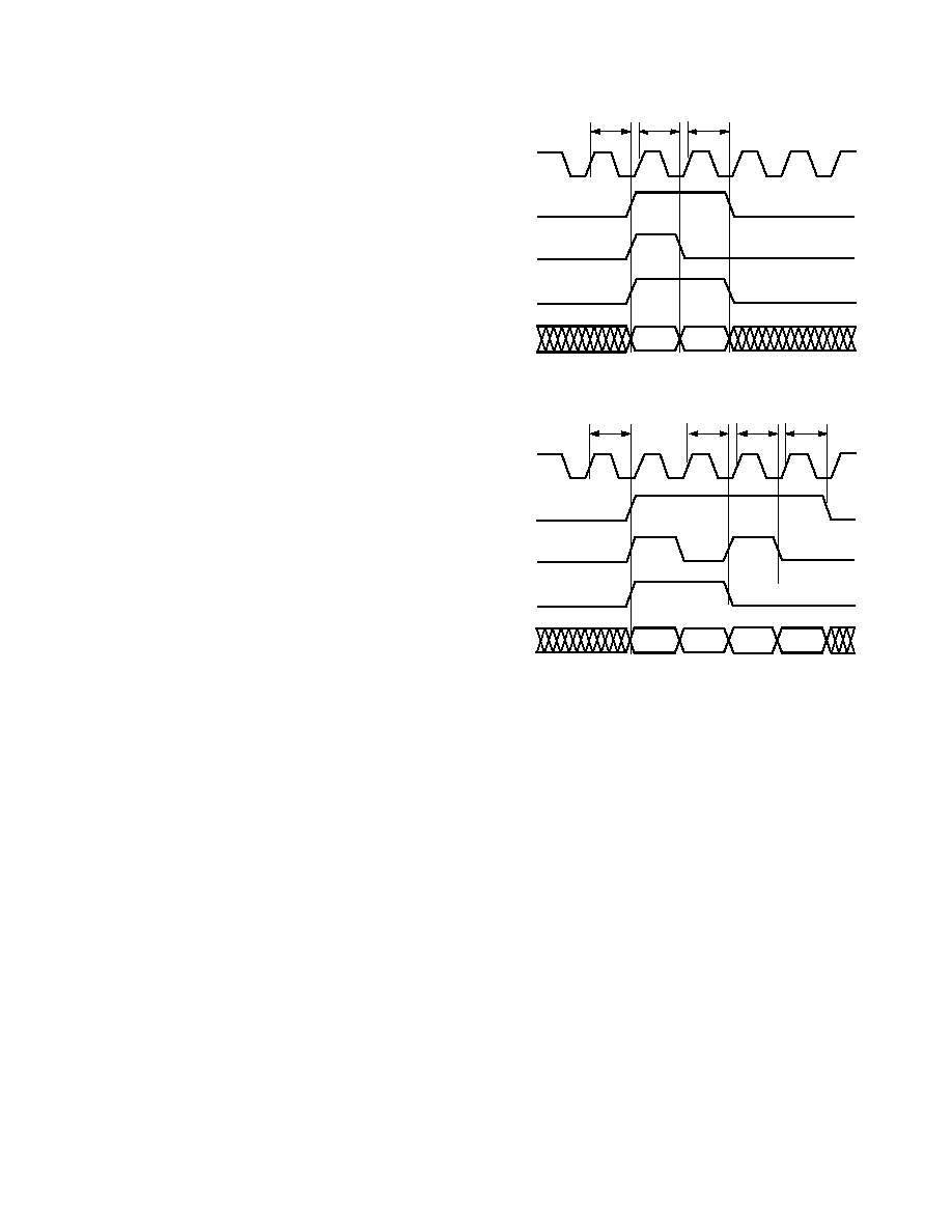
DVOUT
DVOUT is provided to signal that valid data is present. If this pin
is high, there is a valid data word on the bus. DVOUT remains high
for two high-speed clock cycles in Single Channel Real and Single
Channel Complex Mode and for four high-speed clock cycles in
Diversity Channel Real mode. After DVOUT returns low the Q data
will remain until the next data sample.
I/QOUT
When this pin is high the data word represents I data; when
I/QOUT is low Q data is present. This signal will also be low when
DVOUT is low since the last word of every data phase is Q data.
A/BOUT
If DVOUT is low, A/BOUT is always low. When A/BOUT is high, A
Channel data is available on the output. If DVOUT remains high
while A/BOUT is low, then B Channel data is on the output pins
of the chip OUT[15:0].
CLK
OUT[15:0]
VALID DATA
A DATA
tDPR
tDPF
IQ
IA
QA
DVOUT
I/QOUT
A/BOUT
Figure 28. Parallel Output Data Timing (Single-Channel
Mode)
tDPR
tDPF
IQ
IA
QA
IB
QB
VALID DATA
A DATA
B DATA
CLK
OUT[15:0]
DVOUT
I/QOUT
A/BOUT
Figure 29. Parallel Output Data Timing (Diversity Channel
Mode)
Serial Output Data Port
The AD6620 provides a choice of two output ports: a 16-bit
parallel port and a synchronous serial port. The advantage of
using the serial port is that all 23 bits of available data can be
output in the 24-bit or 32-bit mode. The serial output port
shares some of the same pins used by the parallel output port.
As a result, one or the other mode of output may be utilized,
but not both. The output mode must be set with a hard reset
generated by at least a 30 ns low time on the
RESET pin. If the
PAR/SER line is low (Logic “0”) upon reset, then serial output
data is activated. The PAR/SER pin should remain static after
the output mode has been set (i.e., PAR/SER should only change
when
RESET is low).
Note that the AD6620 cannot be booted through the serial port.
The microport must be used to initialize the device, then serial
operation is supported.
Figure 30 shows the typical interconnections between an AD6620
in serial master mode and a DSP. Refer to the Serial Control
Port section for a detailed description of pin functions and pro-
cedures for writing and reading with relation to the serial port.
Note the 10 k
resistors connected to SDI and SDO. These
prevent the lines from toggling when the AD6620 or DSP
three-states these pins.
相关PDF资料 |
PDF描述 |
|---|---|
| 6274291-2 | CONN JACK VERT PCB 75 OHM BNC |
| AD7669JNZ | IC I/O PORT 8BIT ANLG 28DIP |
| D38999/24FF11PA | CONN RCPT 11POS JAM NUT W/PINS |
| D38999/20JE26HN | CONN RCPT 26POS WALL MNT W/PINS |
| AD7569KNZ | IC I/O PORT 8BIT ANALOG 24DIP |
相关代理商/技术参数 |
参数描述 |
|---|---|
| AD6620PCB | 制造商:AD 制造商全称:Analog Devices 功能描述:65 MSPS Digital Receive Signal Processor |
| AD6620S | 制造商:AD 制造商全称:Analog Devices 功能描述:65 MSPS Digital Receive Signal Processor |
| AD6620S/PCB | 制造商:Analog Devices 功能描述:DUAL CHANNEL DECIMATING RECEIV 制造商:Analog Devices 功能描述:SGNL PROCESSOR 169CSPBGA - Bulk |
| AD6622 | 制造商:AD 制造商全称:Analog Devices 功能描述:Four-Channel, 75 MSPS Digital Transmit Signal Processor TSP |
| AD6622AS | 制造商:Analog Devices 功能描述:Transmit Signal Processor 128-Pin MQFP 制造商:Rochester Electronics LLC 功能描述:4 CHANNEL 65 MSPS DIGITAL UPCONVERTER - Bulk |
发布紧急采购,3分钟左右您将得到回复。