- 您现在的位置:买卖IC网 > PDF目录11767 > AD6620ASZ-REEL (Analog Devices Inc)IC DGTL RCVR DUAL 67MSPS 80-PQFP PDF资料下载
参数资料
| 型号: | AD6620ASZ-REEL |
| 厂商: | Analog Devices Inc |
| 文件页数: | 7/44页 |
| 文件大小: | 0K |
| 描述: | IC DGTL RCVR DUAL 67MSPS 80-PQFP |
| 标准包装: | 500 |
| 接口: | 并行/串行 |
| 电源电压: | 3 V ~ 3.6 V |
| 封装/外壳: | 80-BQFP |
| 供应商设备封装: | 80-PQFP(14x14) |
| 包装: | 带卷 (TR) |
| 安装类型: | 表面贴装 |
第1页第2页第3页第4页第5页第6页当前第7页第8页第9页第10页第11页第12页第13页第14页第15页第16页第17页第18页第19页第20页第21页第22页第23页第24页第25页第26页第27页第28页第29页第30页第31页第32页第33页第34页第35页第36页第37页第38页第39页第40页第41页第42页第43页第44页
AD6620
–15–
REV. A
INPUT DATA PORT
The input data port accepts a clock (CLK), a 16-bit mantissa
IN[15:0], a 3-bit exponent EXP[2:0], and channel select Pin A/B.
These pins allow direct interfacing to both standard fixed-point
ADCs such as the AD9225 and AD6640, as well as to gain-
ranging ADCs such as the AD6600. These inputs are not 5 V
tolerant and the ADC I/O should be set to 3.3 V.
The input data port accepts data in one of three input modes:
Single Channel Real, Diversity Channel Real, or Single Channel
Complex. The input mode is selected by programming the Input
Mode Control Register located at internal address space 300h.
Single Channel Real mode is used when a single channel ADC
drives the input to the AD6620. Diversity Channel Real mode is
the two channel mode used primarily for diversity receiver appli-
cations. Single Channel Complex mode accepts complex data in
conjunction with the A/B input which identifies in-phase and
quadrature samples (primarily for cascaded 6620s).
The input data port is sampled on the rising edge of CLK at a
maximum rate of 67 MSPS. The 16-bit mantissa, IN[15:0] is
interpreted as a twos complement integer. For most applications
with ADCs having fewer than 16 bits, the active bits should be
MSB justified and the unused LSBs should be tied low.
The 3-bit exponent, EXP[2:0] is interpreted as an unsigned
integer. The exponent can be modified by the 3-bit exponent
offset ExpOff (Control Register 0x305, Bits (7–5)) and an expo-
nent invert ExpInv (Control Register 0x305, Bit 4).
ExpOff sets the offset of the input exponent, EXP[2:0]. ExpInv
determines the direction of this offset. Equations below show
how the exponent is handled.
scaled input
IN
ExpInv
Exp ExpOff
_,
– mod(
, )
=×
=
+
20
8
scaled input
IN
ExpInv
Exp ExpOff
_,
– mod( –
,)
=×
=
+
21
78
where: IN is the value of IN[15:0], Exp is the value of EXP[2:0],
and ExpOff is the value of ExpOff.
Input Scaling
In general there are two reasons for scaling digital data. The
first is to avoid “clipping” or, in the case of the AD6620 regis-
ter, “wrap-around” in subsequent stages. Wrap-around is not a
concern for the input data since the NCO is designed to accept
the largest possible input at the AD6620 data port.
The second use of scaling is to preserve maximum dynamic
range through the chip. As data flows from one stage to the next
it is important to keep the math functions performed in the
MSBs. This will keep the desired signal as far above the noise
floor as possible, thus maximizing signal-to-noise ratio.
Scaling with Fixed-Point ADCs
For fixed-point ADCs, the AD6620 exponent inputs EXP[2:0]
are typically not used and should be tied low. The ADC outputs
are tied directly to the AD6620 Inputs, MSB-justified. The
exponent offset (ExpOff) and exponent invert (ExpInv) should
both be programmed to 0. Thus the input equation,
scaled input
IN
ExpInv
Exp ExpOff
_,
– mod(
, )
=×
=
+
20
8
where: IN is the value of IN[15:0], Exp is the value of EXP[0:2],
and ExpOff is the value of ExpOff, simplifies to,
scaled
input
IN
_
– mod( , )
=× 2
08
Thus for fixed-point ADCs, the exponents are typically static
and no input scaling is used in the AD6620.
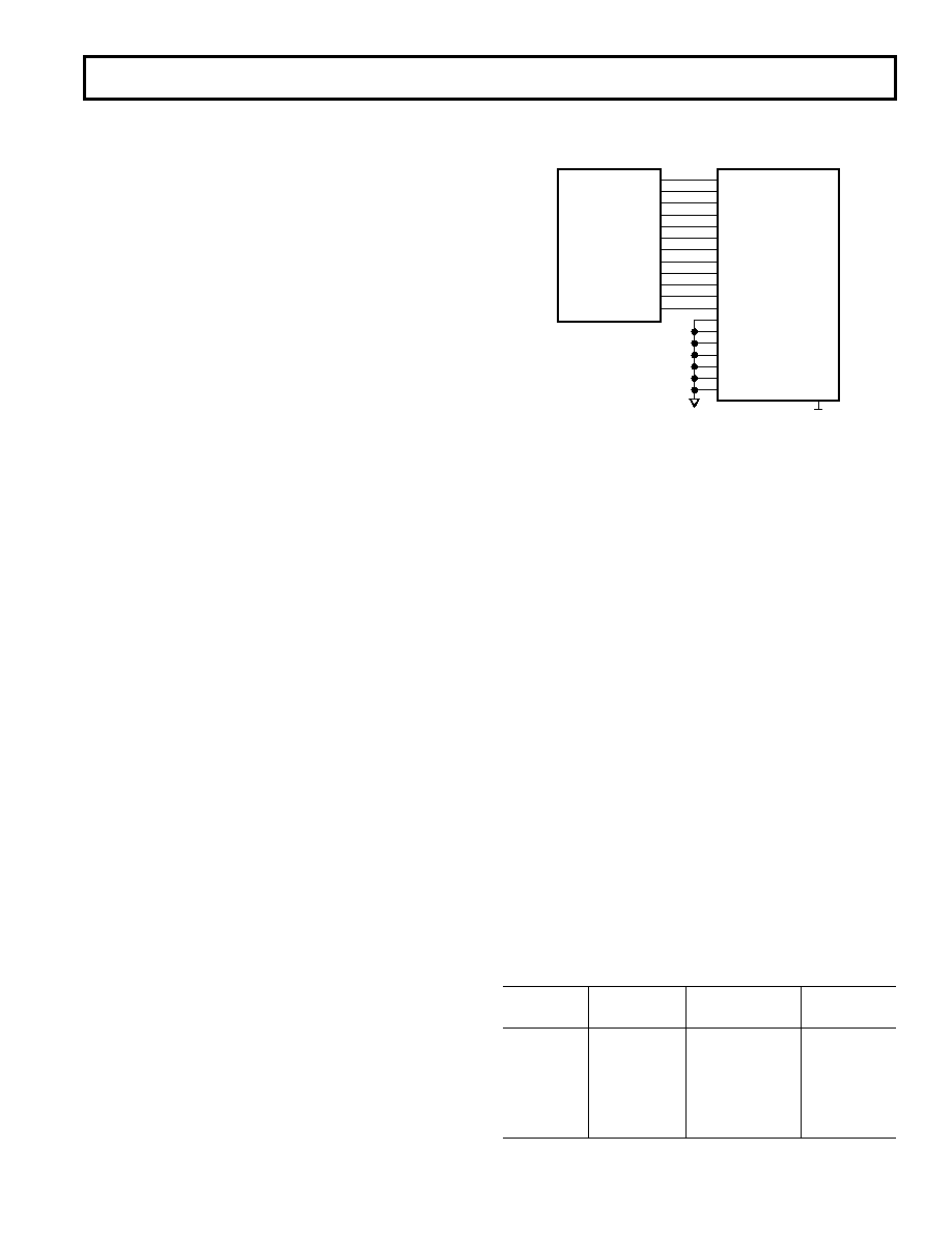
IN4
IN3
IN2
IN1
IN0
EXP2
EXP1
EXP0
IN15
D11 (MSB)
D0 (LSB)
AD6640
AD6620
A/B
+3.3V
Figure 21. Typical Interconnection of the AD6640 Fixed
Point ADC and the AD6620
Scaling with Floating-Point ADCs
An example of the exponent control feature combines the AD6600
and the AD6620. The AD6600 is an 11-bit ADC with three bits
of gain ranging. In effect, the 11-bit ADC provides the mantissa,
and the three bits of relative signal strength indicator (RSSI) are
the exponent. Only five of the eight available steps are used by
the AD6600. See the AD6600 data sheet for additional details.
For gain-ranging ADCs such as the AD6600,
scaled input
IN
ExpInv
Exp ExpOff
_,
– mod( –
,)
=×
=
+
21
78
where: IN is the value of IN[15:0], Exp is the value of EXP[2:0],
and ExpOff is the value of ExpOff.
The RSSI output of the AD6600 numerically grows with increas-
ing signal strength of the analog input (RSSI = 5 for a large
signal, RSSI = 0 for a small signal). With the Exponent Offset
equal to zero and the Exponent Invert Bit equal to zero, the
AD6620 would consider the smallest signal at the parallel input
(EXP = 0) the largest and, as the signal and EXP word increase,
it shifts the data down internally (EXP = 5, will shift the 11-bit
data right by 5 bits internally before going into the CIC2). The
AD6620 regards the largest signal possible on the AD6600 as
the smallest signal. Thus the Exponent Invert Bit is used to make
the AD6620 exponent agree with the AD6600 RSSI. When it
is set high, it forces the AD6620 to shift the data up for growing
EXP instead of down. The exponent invert bit should always be
set high for use with the AD6600.
Table I. AD6600 Transfer Function with AD6620 ExpInv = 1,
and No ExpOff
ADC Input
AD6600
AD6620
Signal
Level
RSSI[2.0]
Data
Reduction
Largest
101 (5)
4 (>> 2)
–12 dB
100 (4)
8 (>> 3)
–18 dB
011 (3)
16 (>> 4)
–24 dB
010 (2)
32 (>> 5)
–30 dB
001 (1)
64 (>> 6)
–36 dB
Smallest
000 (0)
128 (>> 7)
–42 dB
(ExpInv = 1, ExpOff = 0)
相关PDF资料 |
PDF描述 |
|---|---|
| 6274291-2 | CONN JACK VERT PCB 75 OHM BNC |
| AD7669JNZ | IC I/O PORT 8BIT ANLG 28DIP |
| D38999/24FF11PA | CONN RCPT 11POS JAM NUT W/PINS |
| D38999/20JE26HN | CONN RCPT 26POS WALL MNT W/PINS |
| AD7569KNZ | IC I/O PORT 8BIT ANALOG 24DIP |
相关代理商/技术参数 |
参数描述 |
|---|---|
| AD6620PCB | 制造商:AD 制造商全称:Analog Devices 功能描述:65 MSPS Digital Receive Signal Processor |
| AD6620S | 制造商:AD 制造商全称:Analog Devices 功能描述:65 MSPS Digital Receive Signal Processor |
| AD6620S/PCB | 制造商:Analog Devices 功能描述:DUAL CHANNEL DECIMATING RECEIV 制造商:Analog Devices 功能描述:SGNL PROCESSOR 169CSPBGA - Bulk |
| AD6622 | 制造商:AD 制造商全称:Analog Devices 功能描述:Four-Channel, 75 MSPS Digital Transmit Signal Processor TSP |
| AD6622AS | 制造商:Analog Devices 功能描述:Transmit Signal Processor 128-Pin MQFP 制造商:Rochester Electronics LLC 功能描述:4 CHANNEL 65 MSPS DIGITAL UPCONVERTER - Bulk |
发布紧急采购,3分钟左右您将得到回复。